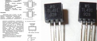
It is not known who was the first to come up with the idea of making two or more transistors on one semiconductor chip. Perhaps this idea arose immediately after the start of production of semiconductor elements. It is known that the theoretical foundations of this approach were published in the early 50s of the last century. It took less than 10 years to overcome technological problems, and already in the early 60s the first device was released containing several electronic components in one housing - a microcircuit (chip). From that moment on, humanity embarked on a path of improvement that has no end in sight.
Story
The invention of microcircuits began with the study of the properties of thin oxide films, which manifest themselves in the effect of poor electrical conductivity at low electrical voltages.
The problem was that where the two metals touched, there was no electrical contact or it was polar. Deep studies of this phenomenon led to the discovery of diodes and later transistors and integrated circuits. In 1958, two scientists living in completely different places invented an almost identical integrated circuit model. One of them, Jack Kilby, worked for Texas Instruments, the other, Robert Noyce, was one of the founders of the small semiconductor manufacturing company Fairchild Semiconductor. Both were united by the question: “How to fit a maximum of components into a minimum of space?” Transistors, resistors, capacitors and other parts were placed separately on boards at that time, and scientists decided to try to combine them on one monolithic chip made of semiconductor material. Only Kilby used germanium, and Noyce preferred silicon. In 1959, they separately received patents for their inventions - a confrontation between the two companies began, which ended with a peace treaty and the creation of a joint license for the production of chips. After Fairchild Semiconductor Corporation made integrated circuits commercially available in 1961, they were immediately used in the production of calculators and computers instead of individual transistors, allowing for significant reduction in size and increased performance.
The first Soviet semiconductor microcircuit was created in 1961 at the Taganrog Radio Engineering Institute, in the laboratory of L. N. Kolesov.
The first semiconductor integrated circuit in the USSR was developed (created) on the basis of planar technology developed at the beginning of 1960 at NII-35 (then renamed the Pulsar Research Institute) by a team that was later transferred to NIIME (Mikron). The creation of the first domestic silicon integrated circuit was concentrated on the development and production with military acceptance of the TC-100 series of integrated silicon circuits (37 elements - the equivalent of the circuit complexity of a flip-flop, an analogue of the American IC series SN-51 from Texas Instruments). Prototype samples and production samples of silicon integrated circuits for reproduction were obtained from the USA. The work was carried out by NII-35 (director Trutko) and the Fryazino plant (director Kolmogorov) under a defense order for use in an autonomous altimeter of a ballistic missile guidance system. The development included six standard integrated silicon planar circuits of the TS-100 series and, with the organization of pilot production, took three years at NII-35 (from 1962 to 1965). It took another two years to develop factory production with military acceptance in Fryazino (1967).
Integrated Circuit Design Idea
The idea behind a chip was to take the complete circuit, with all its many electronic components and connections, and then recreate it in microscopic form on the surface of a piece of silicon. Thanks to this idea, all sorts of “microelectronic” gadgets emerged that are now taken for granted:
- digital clock,
- pocket calculators,
- space rockets,
- satellite navigation and much more.
Integrated circuits revolutionized electronics and computing during the 1960s and 1970s. Gradually, integrated circuits were modernized, which was accompanied by an increase in the scale of integration of electronic components while maintaining (and even reducing) small overall dimensions:
- Small Scale Integration (SSI)
- Medium Scale Integration (MSI)
- Large Scale Integration (LSI)
- Very Large Scale Integration (VLSI)
- Ultra Large Scale Integration (ULSI)
Structured integrated circuit inside a chip
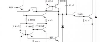
So, the process of creating an integrated circuit begins with a single silicon crystal, shaped like a long solid pipe, “cut” into thin disks - plates. Such wafers are laid out into many identical square or rectangular areas, each of which represents one silicon chip (microchip). An example of the internal structure of an integrated circuit, demonstrating the capabilities of such a unique technology for integrating full-fledged electronic circuit solutions.
It will be interesting➡ All about power supplies - device diagram, DIY production
Thousands, millions, or even billions of components are then created on each chip by doping different areas of the surface into N-type or P-type silicon. Alloying is carried out in various ways. One option is sputtering, when a silicon wafer is “bombarded” with ions of the dopant material.
Another option is vapor deposition, which involves introducing an alloying material in the gas phase followed by condensation. As a result of this introduction, impurity atoms form a thin film on the surface of the silicon wafer. Molecular beam epitaxy is considered the most accurate deposition option.
Of course, the creation of integrated circuits, where hundreds, millions or billions of components are packed into a silicon chip the size of a fingernail, seems to be a very complex process. One can imagine what chaos even a small grain will bring when working on a microscopic (nanoscopic) scale. This is why semiconductors are manufactured in squeaky clean laboratory conditions. The air in laboratory rooms is carefully filtered, and workers must pass through protective airlocks and wear protective clothing.
Interesting read: what are klystrons.
Who created the integrated circuit?
The development of the integrated circuit is credited to two physicists, Jack Kilby and Robert Noyce, as a joint invention. However, in fact, Kilby and Noyce hatched the idea of an integrated circuit independently of each other. There was even a kind of competition between scientists for the rights to the invention.
Jack Kilby was working at Texas Instruments when the scientist managed to realize the idea of a monolithic principle of placing various parts of an electronic circuit on a silicon chip. The scientist manually created the world's first integrated circuit (1958), using a germanium-based chip. a year later she filed a patent application.
Meanwhile, a representative of the other, Robert Noyce, conducted experiments with miniature circuits of his device. Through a series of photographic and chemical techniques (the planar process), Kilby created a practical integrated circuit just a year later. The production method was also filed for a patent.
Microcircuits on the board
What are Logic Integrated Circuits (ICs)
Essentially, this is a microelectronic device that is based on a crystal of arbitrary complexity, which is made on a semiconductor film or wafer. It is placed in a non-separable case (although it can do without it, but only when it is part of a microassembly). The first integrated circuit was patented in 1968. This was a kind of breakthrough in the industry, although the provided device did not very much correspond to modern ideas in its parameters. Integrated circuits are mostly manufactured for surface mounting. Often, IC is understood as just one crystal or film. The most widespread is the integrated circuit on a silicon wafer. It so happens that its use in industry has a number of advantages, for example, the efficiency of signal transmission.
Brief historical background.
The first experiments in creating semiconductor integrated circuits were carried out in 1953, and industrial production of integrated circuits began in 1959. In 1966, production of integrated circuits of medium degree of integration began (the number of elements in one crystal is up to 1000). In 1969, integrated circuits with a higher degree of integration (large-scale integrated circuits, LSI) were created, containing up to 10,000 elements in one chip.
Vasiliev Dmitry Petrovich
Professor of Electrical Engineering, St. Petersburg State Polytechnic University
Ask a Question
In 1971, microprocessors were developed, and in 1975, very-large-scale integrated circuits (VLSI), containing more than 10,000 elements in a single chip. It is useful to note that the limiting frequency of bipolar transistors in semiconductor integrated circuits reaches 15 GHz or more.
By 2000, integrated circuits are expected to appear containing up to 100 million MOS transistors in a single chip (we are talking about digital circuits).
What is an integrated circuit
An integrated circuit is a miniature electronic unit containing in a common housing transistors, diodes, resistors and other active and passive elements, the number of which can reach several tens of thousands.
One microcircuit can replace an entire unit of a radio receiver, an electronic computer (computer) and an electronic machine. The “mechanism” of a digital wristwatch, for example, is just one larger chip.
According to their functional purpose, integrated circuits are divided into two main groups: analog, or linear-pulse, and logical, or digital, microcircuits.
Analog microcircuits are intended for amplification, generation and conversion of electrical oscillations of different frequencies, for example, for receivers, amplifiers, and logical ones - for use in automation devices, in devices with digital timekeeping, in computers.
This workshop is devoted to familiarization with the device, operating principle and possible application of the simplest analog and logical integrated circuits.
Purpose of microcircuits
Currently, a wide variety of electronic components with varying degrees of integration are manufactured in an integrated design. From them, like from cubes, you can assemble various electronic devices. Thus, the radio receiver circuit can be implemented in various ways. The initial option is to use microcircuit sets of transistors. By connecting their terminals, you can create a receiving device. The next stage is to use individual units in an integrated design (each in its own housing):
- radio frequency amplifier;
- heterodyne;
- mixer;
- audio amplifier.
Finally, the most modern option is the entire receiver in one chip, you just need to add a few external passive elements. Obviously, as the degree of integration increases, the construction of circuits becomes simpler. Even a full-fledged computer can now be implemented on a single chip. Its performance will still be lower than that of conventional computing devices, but with the development of technology, perhaps this point will be overcome.
Design Levels
- Physical - methods of implementing one transistor (or a small group) in the form of doped zones on a crystal.
- Electrical - circuit diagram (transistors, capacitors, resistors, etc.).
- Logical - logical circuit (logical inverters, OR-NOT, AND-NOT elements, etc.).
- Circuit and system level - circuit and system design (flip-flops, comparators, encoders, decoders, ALUs, etc.).
- Topological - topological photomasks for production.
- Program level (for microcontrollers and microprocessors) - assembler instructions for the programmer.
Currently, most integrated circuits are developed using CAD systems, which make it possible to automate and significantly speed up the process of obtaining topological photomasks.
How are integrated circuits created?
How to make a memory chip or computer processor? The manufacturing process begins with the chemical element silicon, which is chemically treated (alloyed) to impart different electrical properties.
MEMORY CHIP
A modern design of an integrated circuit (one of many forms) installed on the electronic board of the device. This is far from the most advanced option, but only one of many
Traditionally, materials of two categories are used for electronics needs:
- Conductors.
- Insulators.
But technically, everything is more complicated, especially when it comes to certain elements in the middle of the periodic table (groups 14 and 15), in particular silicon and germanium. What is noteworthy is that insulating materials can become conductors if a certain amount of impurities is added to these materials. A process known as alloying.
PLCC housing
PLCC ( Plastic L eaded C hip C arrier) and CLCC ( C eramic L eaded C hip C contacts located along the edges, designed for installation in a special socket, popularly called a “crib”. A typical example is the BIOS chip in your computers.
This is what the “bed” for such microcircuits looks like:
And this is how the microcircuit “lies” in the crib.
Sometimes such chips are called QFJ , as you guessed it, because of the “J”
Well, the number of pins is placed after the name of the case, for example PLCC32.
Production.
Manufacturing an integrated circuit can take up to two months because certain areas of the semiconductor must be precisely doped. In a process called crystal growing, or crystal pulling, a cylindrical slab of high-purity silicon is first produced. From this cylinder, plates with a thickness of, for example, 0.5 mm are cut. The wafer is eventually cut into hundreds of small pieces called chips, each of which is transformed into an integrated circuit through the process described below.
The chip processing process begins with the production of masks for each layer of the IC. A large-scale stencil is made, shaped like a square with an area of approx. 0.1 m2. A set of such masks contains all the components of the IC: diffusion levels, interconnect levels, etc. The entire resulting structure is photographically reduced to the size of a crystal and reproduced layer by layer on a glass plate. A thin layer of silicon dioxide is grown on the surface of the silicon wafer. Each plate is coated with a light-sensitive material (photoresist) and exposed to light transmitted through masks. Unexposed areas of the photosensitive coating are removed with a solvent, and with the help of another chemical reagent that dissolves silicon dioxide, the latter is etched from those areas where it is no longer protected by the photosensitive coating. Variations of this basic process technology are used in the fabrication of two main types of transistor structures: bipolar and field-effect (MOS).
SOP housing
SOP ( Small Outline Package - the same as SOIC .
SOP housing modifications:
PSOP - plastic SOP housing. Most often this is what is used.
HSOP is a heat dissipating SOP. Small radiators in the middle serve to remove heat.
SSOP ( Shrink S mall O utline Package ) - “shrinked” SOP . That is, even smaller than the SOP housing
TSSOP ( Thin S hrink S mall O utline Package ) - thin SSOP . The same SSOP, but “smeared” with a rolling pin. Its thickness is less than that of SSOP. Basically, microcircuits are made in TSSOP packages, which get quite hot. Therefore, the area of such microcircuits is larger than that of conventional ones. In short, a radiator housing).
SOJ is the same SOP, but the legs are bent in the shape of the letter “J” under the chip itself. SOJ body was named after these legs :
Well, as usual, the number of pins is indicated after the package type, for example SOIC16, SSOP28, TSSOP48, etc.
Main types of modern microcircuits
It is important to understand that progress does not stand still: every year the list of main types of microcircuits undergoes significant changes, in addition, their range is expanding.
The types of microcircuits are different, depending on the main evaluation criteria.
By purpose:
1. Digital. Necessary for processing a special signal expressed in digital code. They have a significant number of advantages over other types: lower costs for electricity consumption, in addition, they have greater resistance to interference.
Digital microcircuits are often used in various computers, such as automation systems, electronic computers and many others.
2. Analog. Designed for processing and converting continuously incoming signals. Analog chips have high performance. Often used in such popular devices as:
Video recorders.
Televisions.
Audio frequency converters.
In various voltage stabilizers.
In sensors.
Operational amplifiers.
3. Analog-digital. They are a true hybrid of the two microcircuits presented above. They are very popular due to their increased performance indicators; in addition, they combine the positive characteristics of two types of microcircuits at once. They are used to create most modern technology, such as:
Modulators and demodulators.
Switches.
Frequency generators and restorers.
By type of construction:
1. Film. These are microcircuits for the manufacture of which a special technique is used. In addition, all connecting elements are a special film layer. There are certain divisions into two types: thin-film and thick-film, differing in the thickness of the film layer.
2. Semiconductor chips are not used very often; they are made using plastic (usually epoxy resin) with special wire or tape leads that ensure the performance of the device.
3. Hybrid. More complex devices, for the manufacture of which not only popular films and substrates are used, but also less common attachment materials (for example, various crystals).
By body type:
1. Cabinet. With this type of design, the microcircuit is placed in a special case (the material from which it is made can be chosen by the manufacturer). This type is not particularly popular in everyday life. Most often, the microcircuit is placed in a housing in order to avoid breakage or deformation of individual parts during transportation.
Packaged microcircuits are used to transport large quantities of goods. In any other case, it is cheaper for the manufacturer to produce unpackaged microcircuits.
2. Unpackaged microcircuits. Most often, it is the open-frame models that are used. The microcircuit does not fit into the case; in this case, for protection, all parts are filled with special paint or compound. This is what allows you to protect the crystal from damage or any other negative environmental influences.
Such designs are produced specifically for installation in a hybrid circuit or preliminary microassembly.
When choosing a microcircuit, you should take into account all the advantages and disadvantages of the main types. Certain technical devices require certain microcircuits; in order to select the required model, it is necessary to obtain professional advice from specialists in this field. In this case, the device you choose will last a long time.
SOIC package
The largest representative of this class of microcircuits are microcircuits in the SOIC ( S mall - Outline I ntegrated C circuit) - a small microcircuit with pins on the long sides. It is very similar to DIP, but pay attention to its conclusions. They are parallel to the surface of the body itself:
This is how they are soldered on the board:
Well, as usual, the number after “SOIC” indicates the number of pins of this microcircuit. The photo above shows microcircuits in the SOIC16 package.
Purpose
An integrated circuit can have complete, no matter how complex, functionality - up to an entire microcomputer (single-chip microcomputer).
Analog circuits
- Operational amplifiers
- Signal generators
- Filters (including piezoelectric effect)
- Analog multipliers
- Analog attenuators and variable amplifiers
- Power supply stabilizers
- Switching power supply control chips
- Signal converters
- Timing circuits
- Various sensors (temperature, etc.)
Digital circuits
- Logic elements
- Triggers
- Counters
- Registers
- Buffer converters
- Memory modules
- Encryptors
- Decoders
- Microcontrollers
- (Micro)processors (including the CPU in a computer)
- Single-chip microcomputers
- FPGA - programmable logic integrated circuits
Digital integrated circuits have a number of advantages over analog ones:
- Reduced power consumption
is associated with the use of pulsed electrical signals in digital electronics. When receiving and converting such signals, the active elements of electronic devices (transistors) operate in the “key” mode, that is, the transistor is either “open” - which corresponds to a high-level signal (1), or “closed” - (0), in the first case at There is no voltage drop in the transistor; in the second, no current flows through it. In both cases, power consumption is close to 0, in contrast to analog devices, in which most of the time the transistors are in an intermediate (resistive) state. - The high noise immunity
of digital devices is associated with the large difference between high (for example 2.5 - 5 V) and low (0 - 0.5 V) level signals. An error is possible with such interference when a high level is perceived as low and vice versa, which is unlikely. In addition, digital devices can use special codes to correct errors. - The large difference between high and low level signals and a fairly wide range of their permissible changes makes digital technology insensitive
to the inevitable dispersion of element parameters in integrated technology, eliminating the need to select and configure digital devices.
Analog-to-digital circuits
- DAC and ADC
- CVS
- Transceivers (for example, RS422 interface converter)
- Modulators and demodulators Radio modems
- Decoders for teletext, VHF radio text
- Transceivers Fast
- Dial-Up modems
- Digital TV receivers
- Optical mouse sensor
On a logic chip
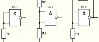
An integral part of many digital integrated circuits is the AND-NOT logical element, the symbol of which you see in Fig. 4, a. Its symbol is the "&" sign placed inside a rectangle, usually in the upper left corner, replacing the conjunction "AND" in English. There are two or more inputs on the left, one output on the right.
The small circle that begins the communication line of the output signal symbolizes the logical Negation “NOT” at the output of the microcircuit. In the language of digital technology, “NOT” means that the NAND element is an inverter, that is, a device whose output parameters are opposite to the input ones.
The electrical state and operation of a logic element are characterized by the signal levels at its inputs and output. A small (or zero) voltage signal, the level of which does not exceed 0.3 - 0.4 V, is usually called (in accordance with the binary number system) logical zero (0), and a higher voltage signal (compared to logical 0), the level of which can be 2.5 - 3.5 V, - logical unit (1).
For example, they say: “the output of the element is logical 1.” This means that at the moment a signal has appeared at the output of the element, the voltage of which corresponds to the logical level 1.
In order not to delve into the technology and structure of the NAND element, we will consider it as a “black box”, which has two inputs and one output for an electrical signal.
The logic of the element is that when logical O is applied to one of its inputs, and logical 1 is applied to the second input, a logical 1 signal appears at the output, which disappears when signals corresponding to logical 1 are applied to both inputs.
For experiments that memorize this property of the element, you will need the most common K155LAZ microcircuit, a DC voltmeter, a fresh 3336L battery and two resistors with a resistance of 1...1.2 kOhm.
Rice. 4. Logical elements of the K155LAZ microcircuit.
The K155LAZ microcircuit consists of four 2I-NOT elements (Fig. 4, b), powered by one common DC source of 5 V, but each of them operates as an independent logical device. The number 2 in the name of the microcircuit indicates that its elements have two inputs.
In appearance and design, it, like all microcircuits of the K155 series, does not differ from the already familiar analog microcircuit K118UN1, only the polarity of connecting the power source is different. Therefore, the cardboard board you made earlier is suitable for experiments with this microcircuit. The power source is connected: +5 V - to pin 7" - 5 V - to pin 14.
But these conclusions are not usually indicated on a schematic diagram of the microcircuit. This is explained by the fact that on circuit diagrams the elements that make up the microcircuit are depicted separately, for example, as in Fig. 4, c. For experiments, you can use any of its four elements.
Solder the microcircuit with pins 1, 7, 8 and 14 to the wire stands on the cardboard board (as in Fig. 1). One of the input pins of any of its elements, for example, an element with pins 1 - 3, is connected through a resistor with a resistance of 1...1.2 kOhm to pin 14, the pin of the second input is directly connected to the common (“grounded”) conductor of the power circuit, and Connect a DC voltmeter to the output of the element (Fig. 5, a).
Turn on the power. What does the voltmeter show? A voltage of approximately 3 V. This voltage corresponds to a logic 1 signal at the output of the element. Using the same voltmeter, measure the voltage at the output of the first input. And here, as you can see, it is also logical 1. Therefore, when one of the inputs of the element is logical 1, and the second is logical 0, the output will be logical 1.
Rice. 5. Voltage measurements on a logic element.
Now connect the output of the second input through a resistor with a resistance of 1...1.2 kOhm to terminal 14 and at the same time with a wire jumper - with a common conductor, as shown in Fig. 5 B.
In this case, the output, as in the first experiment, will be logical 1. Next, watching the voltmeter needle, remove the jumper wire so that a signal corresponding to logical 1 is sent to the second input.
What does a voltmeter record? The signal at the output of the element is converted to logical 0. This is how it should be! And if any of the inputs are periodically shorted to a common wire and thereby simulate the supply of a logical 0 to it, then current pulses will appear at the output of the element with the same frequency, as evidenced by fluctuations in the voltmeter needle. Check this out experimentally.
The property of the NAND element to change its state under the influence of input control signals is widely used in various digital computing devices. Radio amateurs, especially beginners, very often use a logic element as an inverter - a device whose output signal is opposite to the input signal.
The following experiment can confirm this property of the element. Connect the terminals of both inputs of the element together and, through a resistor with a resistance of 1...1.2 kOhm, connect them to pin 14 (Fig. 5, c).
This way you will apply a signal corresponding to logical 1 to the common input of the element, the voltage of which can be measured with a voltmeter. What is the output?
The voltmeter needle connected to it slightly deviated from the zero scale mark. Here, therefore, as expected, the signal corresponds to logical 0.
Then, without disconnecting the resistor from pin 14 of the microcircuit, connect the input of the element to the common conductor with a wire jumper several times in a row (shown in Fig. 5, c by a dashed line with arrows) and at the same time watch the voltmeter arrow.
So you will be convinced that when the inverter input is logical 0, the output is logical 1 and, conversely, when the input is logical 1, the output is logical 0.
This is how an inverter works, especially often used by radio amateurs in the pulse devices they construct.
Rice. 6. Circuit diagram of an AF signal generator on a microcircuit.
An example of such a device is a pulse generator assembled according to the circuit shown in Fig. 6. You can verify its functionality right away, spending just a few minutes on it.
The output of element D1.1 is connected to the inputs of element D1.2 of the same microcircuit, its output is connected to the inputs of element DJ.3, and the output of this element (output ) is connected to the input of element D1.1 through a variable resistor R1. To the output of element D1.3 (between pin 8 and the common conductor) connect headphones B1, and electrolytic capacitor C1 in parallel with elements D1.1 and D1.2.
Set the variable resistor motor to the right (according to the diagram) position and turn on the power - you will hear a sound in the phones, the tone of which can be changed with a variable resistor.
In this experiment, elements D1.1, D1.2 and D1.3, connected in series, like transistors of a three-stage amplifier, formed a multivibrator - a generator of rectangular electrical pulses.
The microcircuit became a generator thanks to a capacitor and resistor, which created frequency-dependent feedback circuits between the output and input of the elements. Using a variable resistor, the frequency of the pulses generated by the multivibrator can be smoothly varied from approximately 300 Hz to 10 kHz.
What practical application can such a pulse device find? It can become, for example, an apartment bell, a probe for checking the performance of the receiver and low-frequency amplifier cascades, a generator for training in listening to the telegraph alphabet.
Chip series
Analog and digital microcircuits are produced in series. A series is a group of microcircuits that have a single design and technological design and are intended for joint use. Microcircuits of the same series, as a rule, have the same power supply voltages and are matched in terms of input and output resistances and signal levels.
Housings
Integrated circuit housings designed for surface mounting A microassembly with a packageless microcircuit welded onto a printed circuit board.
A microcircuit housing is a structure designed to protect the microcircuit crystal from external influences, as well as for ease of installation of the microcircuit into an electronic circuit. It contains the housing itself made of dielectric material (plastic, less often ceramic), a set of conductors for electrically connecting the crystal with external circuits through leads, and markings.
There are many options for microcircuit packages, differing in the number of microcircuit pins, installation method, and operating conditions. To simplify installation technology, chip manufacturers are trying to unify packages by developing international standards.
Sometimes microcircuits are produced in an unpackaged design - that is, a crystal without protection. Packless microcircuits are usually designed for installation in a hybrid microassembly. For mass-produced cheap products, direct mounting on a printed circuit board is possible.
Microcircuit in a radio receiver
We propose to test this microcircuit in the high-frequency path of a receiver assembled, for example, according to the circuit shown in Fig. 3. The input circuit of the magnetic antenna of such a receiver is formed by coil L1 and variable capacitor C1. The high-frequency signal of the radio station to which the circuit is tuned is sent through the coupling coil L2 and the separating capacitor C2 to the input (pin 3) of the L1 microcircuit.
From the output of the microcircuit (pin 10, connected to pin 9), the amplified signal is fed through capacitor C4 to the detector, diodes VI and V2 of which are connected according to the voltage multiplication circuit, and the low-frequency signal allocated to it is converted into sound by phones B1. The receiver is powered by a GB1 battery, composed of four 332, 316 cells or five D-01 batteries.
Rice. 3. Receiver circuit on a microcircuit.
In many transistor receivers, the high-frequency amplifier is formed by transistors, but in this one it is a microcircuit. This is the only difference between them.
Having the experience of previous workshops, I hope you will be able to independently mount and set up such a receiver and even, if you wish, supplement it with a low-frequency amplifier for loud-speaking radio reception.
World market
In 2022, the global integrated circuit market was valued at $700 billion.
The main producers and exporters are in Asia: Singapore ($115 billion), South Korea ($104 billion), China ($80.1 billion) and Malaysia ($55.7 billion). The largest European exporter is Germany ($1.4 billion), the American exporter is the USA ($28.9 billion). The largest importers: China ($207 billion), Hong Kong ($168 billion), Singapore ($57.8 billion), South Korea ($38.6 billion) and Malaysia ($37.3 billion).
LGA case
LGA ( L and G rid A rray) is a type of microcircuit package with a matrix of contact pads. Most often used in computer technology for processors.
The crib for LGA chips looks something like this:
If you look closely, you can see spring-loaded contacts.
The chip itself, in this case the PC processor, simply has metallized pads:
In order for everything to work, a condition must be met: the microprocessor must be pressed tightly to the crib. Various types of latches are used for this.
Legal Features
What does the law say about integrated circuits? Our country provides legal protection for integrated circuit topologies. By it we mean the geometric-spatial arrangement of a certain set of specific elements and connections between them, recorded on a certain material medium (according to Article 1448 of the Civil Code of the Russian Federation). The author of the topology has the following intellectual rights to his invention:
- Copyright.
- Exclusive right.
In addition, the author of the topology may have other preferences, including the possibility of receiving remuneration for its use. The exclusive right is valid for ten years. During this time, the inventor, or the person to whom this status has been assigned, can register the topology with the appropriate intellectual property and patent service.
PGA package
PGA ( P in G rid A rray) - a matrix of pin pins. It is a rectangular or square case, in the lower part of which there are pins.
Such microcircuits are also installed in special cribs, which clamp the terminals of the microcircuit using a special lever.
PGA packages are mainly used to make processors for your personal computers.
Radio components in microcircuits containing precious metals
Microcircuits contain many radio components containing precious metals such as gold, silver, platinum and others. They are mainly available in the form of sputtering, and rarely in the form of whole components. The most valuable are the Soviet parts.
A thin layer of gold can be found on contacts and connectors for connecting individual elements.
Transistors, resistors, diodes, and cables are also valuable. After going up for purchase, radio components from microcircuits are sent for recycling. It’s easy to hand over radio components in Moscow, just contact our specialists. ◄ Back to news
