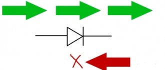
What is the difference between forward and reverse bias?
Applying a voltage to a diode such that the diode begins to pass current is called forward bias. Applying a voltage to a diode such that the diode stops passing current is called reverse biasing.
Interesting materials:
How to recover photos? How to restore WhatsApp function? How to restore gallery on Android? How to restore gallery on Samsung Android? How to restore gallery on Android? How to restore gallery on Samsung? How to restore a gallery on a smartphone? How to recover MBR Master Boot Record? How to recover a voice message on WhatsApp? How to restore government services if there is no number?
What it is
VAC stands for current-voltage characteristic of a diode semiconductor. It reflects the dependence of the current that passes through the pn junction of the diode. The current-voltage characteristic determines the dependence of the current on the magnitude, as well as the polarity of the applied voltage. The current-voltage characteristic has the form of a graph (diagram). This graph looks like this:
I-V characteristic for a diode
For each type of diode, the current-voltage characteristic graph will have its own specific appearance. As you can see, the graph contains a curve. The values of forward current (direct connection) are marked vertically at the top, and in reverse at the bottom. But the horizontal diagram and graph display the voltage, similarly in the forward and reverse directions. Thus, the current-voltage characteristic diagram will consist of two parts:
- upper and right part - the element operates in the forward direction. It reflects the passing current. The line in this part goes sharply upward. It characterizes a significant increase in forward voltage;
- lower left part - the element acts in the opposite direction. It corresponds to the closed (reverse) current through the junction. Here the line runs almost parallel to the horizontal axis. It reflects the slow increase in reverse current.
Note! The steeper the vertical top part of the graph is, and the closer the bottom line is to the horizontal axis, the better the rectifying properties of the semiconductor will be.
It is worth noting that the current-voltage characteristic strongly depends on the ambient temperature. For example, an increase in air temperature can lead to a sharp increase in the reverse current. You can build a current-voltage curve with your own hands as follows:
- take the power supply;
- connect it to any diode (minus to the cathode, plus to the anode);
- We take measurements using a multimeter.
From the data obtained, the current-voltage characteristic for a specific element is constructed. Its diagram or graph may look like this.
Nonlinear current-voltage characteristic
The graph shows the current-voltage characteristic, which in this design is called nonlinear. Let's look at examples of different types of semiconductors. For each individual case, this characteristic will have its own schedule, although they will all be of the same nature with only minor changes.
CVC for shotky
One of the most common diodes today is Schottky. This semiconductor was named after the German physicist Walter Schottky. For Schottky, the current-voltage characteristic will have the following form.
CVC for Schottky
As you can see, Schottky is characterized by a low voltage drop in a direct connection situation. The graph itself is clearly asymmetrical. In the forward displacement zone, an exponential increase in current and voltage is observed. Under reverse and forward bias for a given element, the current in the barrier is due to electrons. As a result, such elements are characterized by rapid action, since there are no diffuse and recombination processes. In this case, the asymmetry of the current-voltage characteristic will be typical for barrier-type structures. Here, the dependence of current on voltage is determined by a change in the number of carriers that take part in charge transfer processes.
Light-emitting diode
The inside is structured completely differently than a diode, but has the same properties. It only glows when current flows in the forward direction. The only difference from a diode is in some characteristics. The most important thing is the forward voltage drop. It is much larger than the 0.65 V of a conventional diode and depends mainly on the color of the LED. Starting from red, whose voltage drop is on average 1.8 V, and ending with a white or blue LED, whose voltage drop is about 3.5 V. However, in the invisible spectrum these values are wider.
In fact, the voltage drop here is the minimum ignition voltage of the diode.
At a lower voltage, there will be no current at the power source and the diode simply will not light up. For powerful lighting LEDs, the voltage drop can be tens of volts, but this only means that there are many series-parallel diode assemblies inside the crystal. But now let's talk about indicator LEDs, as they are the simplest. They are produced in various cases, most often in semi-circular ones, with a diameter of 3, 5, 10 mm.
Any diode glows depending on the current flowing. Essentially it is a current device. The voltage drop is obtained automatically. We set the current ourselves. Modern indicator diodes more or less begin to glow at a current of 1 mA, and at 10 mA they already burn out the eyes. For powerful lighting diodes, you need to look at the documentation.
Application of LED
Having only the appropriate resistor, you can set the desired current through the diode.
Of course, you will also need a constant voltage power supply, for example, a 4.5 V battery or any other power supply. For example, let's set a current of 1 mA through a red LED with a voltage drop of 1.8 V.
The diagram shows the nodal potentials, i.e. voltage relative to zero. A multimeter in dialing mode will best tell us which direction to turn on the LED, since sometimes we come across Chinese LEDs with the legs mixed up. When you touch the multimeter probes in the right direction, the LED should glow faintly.
Since a red LED is used, the resistor will drop 4.5 - 1.8 = 2.7V. This is known from Kirchhoff’s second law: the sum of the voltage drops in successive sections of the circuit is equal to the emf of the battery, i.e. 2.7 + 1.8 = 4.5V. To limit the current to 1 mA, the resistor, according to Ohm's law, must have a resistance R = U / I = 2.7 / 0.001 = 2700 Ohms, where U and I are the voltage across the resistor and the current we need. Don't forget to convert the values to SI units, amperes and volts. Since manufactured resistance ratings are standardized, we will choose the closest standard rating of 3.3 kOhm. Of course, in this case the current will change and it can be recalculated using Ohm’s law I = U / R. But often this is not important.
In this example, the current supplied by the battery is small, so the internal resistance of the battery can be neglected.
With lighting LEDs everything is the same, only the currents and voltages are higher. But sometimes they no longer need a resistor; you need to look at the documentation.
Something else about the LED
In fact, to shine is the main purpose of an LED.
But there is another use. For example, an LED can act as a voltage reference. They are necessary, for example, to obtain current sources. Red LEDs are used as reference voltage sources because they are less noisy. They are included in the diagram in the same way as in the previous example. Since the battery voltage is relatively constant, the current through the resistor and LED is also constant, so the voltage drop remains constant. A tap is made from the anode of the LED, where 1.8V is present, and this reference voltage is used in other parts of the circuit. To more reliably stabilize the current on the LED, with a pulsating voltage from the power source, instead of a resistor, a current source is installed in the circuit. But current sources and voltage reference sources are the topic of another article. Maybe someday I'll write it.
Device
Below is a detailed description of the diode structure; studying this information is necessary for further understanding of the principles of operation of these elements:
- The housing is a vacuum cylinder that can be made of glass, metal or durable ceramic varieties of material.
- inside the cylinder . The first is a heated cathode, which is designed to ensure the process of electron emission. The simplest cathode in design is a filament with a small diameter, which heats up during operation, but today indirectly heated electrodes are more common. They are cylinders made of metal and have a special active layer capable of emitting electrons.
- Inside the indirectly heated there is a specific element - a wire that glows under the influence of electric current, it is called a heater.
- The second electrode is the anode, it is needed to receive the electrons that were released by the cathode. To do this, it must have a potential that is positive relative to the second electrode. In most cases, the anode is also cylindrical.
- Both electrodes of vacuum devices are completely identical to the emitter and base of the semiconductor variety of elements.
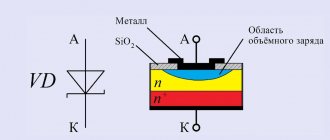
- Silicon or germanium is most often used to make a diode crystal One of its parts is p-type electrically conductive and has a deficiency of electrons, which is formed by an artificial method. The opposite side of the crystal also has conductivity, but it is n-type and has an excess of electrons. There is a boundary between the two regions, which is called a pn junction.
Such features of the internal structure give diodes their main property - the ability to conduct electric current in only one direction.
How to determine voltage and polarity
An LED only allows current to pass in one direction.
Therefore, it is important to connect the device to the circuit correctly. To do this, you need to determine which of the body terminals is the cathode and which is the anode.
- Visually, traditionally the cathode leg is short and the anode leg is long. The cathode has a minus sign, the anode has a plus sign. You can find the cathode in another way. Looking carefully through the case, you can see the crystal on the stand. The output of the stand will be the cathode.
- Connecting to a power source - select a device whose voltage is not higher than the permissible voltage for the LED. Usually this is a battery or resistor. When positioned correctly, the LED glows brighter.
- Using a multimeter - set the scale on the device to resistance measurement mode and touch the leads to the LED terminals with the probes. The contact is very short. When connected in reverse, the multimeter does not show anything; when connected correctly, it measures the resistance in the region of 1.7 kOhm.
Physical and technical parameters
The main parameters of rectifier diodes are based on the following values:
- the maximum permissible value of the potential difference when rectifying the current, at which the device will not fail;
- the highest average rectified current;
- the highest reverse voltage value.
The industry produces rectifiers with different physical characteristics. Accordingly, the devices have different shapes and installation methods. They are divided into three groups:
- High power rectifier diodes. They are characterized by a current capacity of up to 400 A and are high-voltage. High-voltage rectifier diodes are produced in two types of packages - pin, where the case is sealed and glass, and tablet, where the case is made of ceramic.
- Medium power rectifier diodes. They have a capacity from 300 mA to 10A.
- Low power rectifier diodes. The maximum permissible current value is up to 300 mA.
Application areas of diodes
Despite their simple design, semiconductor diodes are widely used in electronics:
- For rectification of alternating voltage. A classic of the genre - the property of a pn junction to conduct current in one direction is used.
- Diode detectors. Here, the nonlinearity of the current-voltage characteristic is used, which makes it possible to isolate harmonics from the signal, the necessary ones of which can be isolated by filters.
- Two diodes connected back-to-back serve as a limiter for powerful signals that can overload subsequent input stages of sensitive radio receiving devices.
- Zener diodes can be switched on as spark-protective elements that prevent high-voltage pulses from entering the circuits of sensors installed in hazardous areas.
- Diodes can serve as switching devices in high-frequency circuits. They open with a constant voltage and allow (or do not allow) the RF signal to pass through.
- Parametric diodes serve as amplifiers of weak signals in the microwave range due to the presence in the forward branch of the characteristic of a section with negative resistance.
- Mixers operating in transmitting or receiving equipment are assembled using diodes. They mix the local oscillator signal with a high-frequency (or low-frequency) signal for subsequent processing. The nonlinearity of the current-voltage characteristic is also used here.
- The nonlinear characteristic allows the use of microwave diodes as frequency multipliers. When a signal passes through a multiplying diode, higher harmonics are released. They can then be identified by filtering.
- Diodes are used as tuning elements in resonant circuits. In this case, the presence of controlled capacitance at the pn junction is used.
- Some types of diodes are used as generators in the microwave range. These are mainly tunnel diodes and devices with the Gunn effect.
This is only a brief description of the capabilities of dual-lead semiconductor devices. With an in-depth study of the properties and characteristics, many problems posed to developers of electronic equipment can be solved using diodes.
Watch this video on YouTube
Operating principle and main characteristics of a zener diode
What is a diode bridge, its operating principle and connection diagram
Description, technical characteristics and analogues of rectifier diodes of the 1N4001-1N4007 series
What is a thyristor, how does it work, types of thyristors and a description of the main characteristics
What is an LED, its operating principle, types and main characteristics
What is a varistor, main technical parameters, what is it used for
Silicon diode and its current-voltage characteristic
In addition to Schottky, silicon semiconductors are very popular at the moment. For a silicon type diode, the current-voltage characteristic looks like this.
I-V characteristics of silicon and germanium diode
For such semiconductors, this characteristic begins at approximately 0.5-0.7 Volts. Very often, silicon semiconductors are compared with germanium semiconductors. If the ambient temperatures are equal, then both devices will exhibit bandgap. In this case, a silicon element will have a lower forward current than one made from germanium. The same rule applies to reverse current. Therefore, germanium semiconductors usually immediately experience thermal breakdown if there is a high reverse voltage. As a result, in the presence of the same temperature and forward voltage, the potential barrier for silicon semiconductors will be higher and the injection current lower.
Basic diode faults
Sometimes devices of this type fail, this may occur due to natural depreciation and aging of these elements or for other reasons.
In total, there are 3 main types of common faults:
- Breakdown of the junction leads to the fact that the diode, instead of a semiconductor device, becomes essentially a very ordinary conductor. In this state, it loses its basic properties and begins to pass electric current in absolutely any direction. Such a breakdown is easily detected using a standard multimeter, which starts beeping and shows a low resistance level in the diode.
- When a break occurs, the reverse process occurs - the device generally stops passing electric current in any direction, that is, it essentially becomes an insulator. To accurately determine a break, it is necessary to use testers with high-quality and serviceable probes, otherwise they can sometimes falsely diagnose this malfunction. In alloy semiconductor varieties, such a breakdown is extremely rare.
- Leakage , during which the tightness of the device body is broken, as a result of which it cannot function properly.
Breakdown of pn junction
Such breakdowns occur in situations where the reverse electric current begins to suddenly and sharply increase, this happens due to the fact that the voltage of the corresponding type reaches unacceptable high values.
There are usually several types:
- Thermal breakdowns , which are caused by a sharp increase in temperature and subsequent overheating.
- Electrical breakdowns that occur under the influence of current on a junction.
The graph of the current-voltage characteristic allows you to visually study these processes and the difference between them.
Electrical breakdown
The consequences caused by electrical breakdowns are not irreversible, since they do not destroy the crystal itself. Therefore, with a gradual decrease in voltage, it is possible to restore all the properties and operating parameters of the diode.
At the same time, breakdowns of this type are divided into two types:
- Tunneling breakdowns occur when high voltage passes through narrow junctions, which allows individual electrons to escape through it. They usually occur if semiconductor molecules contain a large number of different impurities. During such a breakdown, the reverse current begins to increase sharply and rapidly, and the corresponding voltage is at a low level.
- Avalanche types of breakdowns are possible due to the influence of strong fields that can accelerate charge carriers to the maximum level, due to which they knock out a number of valence electrons from atoms, which then fly into the conductive region. This phenomenon is avalanche-like in nature, which is why this type of breakdown received its name.
Thermal breakdown
The occurrence of such a breakdown can occur for two main reasons: insufficient heat removal and overheating of the pn junction, which occurs due to the flow of electric current through it at too high rates.
An increase in temperature in the transition and neighboring areas causes the following consequences:
- The growth of vibrations of the atoms that make up the crystal.
- entering the conductive band.
- A sharp increase in temperature.
- Destruction and deformation of the crystal structure.
- Complete failure and breakdown of the entire radio component.
What does a diode consist of?
In our world there are substances that perfectly conduct electric current. This mainly includes metals, for example, silver, copper, aluminum, gold and so on. Such substances are called conductors. There are substances that conduct electricity very poorly - porcelain, plastics, glass, and so on. They are called dielectrics or insulators. Between conductors and dielectrics are semiconductors. These are mainly germanium and silicon.
Once germanium or silicon is mixed with a minute fraction of arsenic or indium, an N-type semiconductor is formed when mixed with arsenic; or a P-type semiconductor when mixed with indium.
Now if these two P and N type semiconductors are welded together, a PN junction is formed at their junction. This is the structure of a diode. That is, the diode consists of a PN junction.
diode structureThe P-type semiconductor in the diode is the anode, and the N-type semiconductor is the cathode.
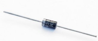
Let's open the Soviet D226 diode and see what's inside it by grinding off part of the body on an emery wheel.
diode D226
This is the same PN junction
PN junction diode