The n-type or p-type semiconductor part is like a resistor, which is not that useful. But when a manufacturer dopes single-crystalline silicon with a p-type material on one side and an n-type material on the other, something new is created: a PN junction.
PN junctions are the elementary building blocks of semiconductor devices such as diodes, transistors, solar cells, LEDs, and integrated circuits. Understanding this allows us to understand the operation of all these devices.
PN junction
Since we know that a p-type semiconductor has trivalent atoms and each of them creates one hole, we can visualize this as shown in the figure below. Each circled minus sign is a trivalent atom, and each plus sign is a hole in its valence orbit.
We also know that n-type semiconductor has pentavalent atoms and each of them produces one free electron, we can visualize this as shown in the following figure. Each circled plus sign is a pentavalent atom, and each minus sign is the free electron it contributes.
A manufacturer can make a single silicon die with p-type material on one side and n-type material on the other side, as shown in the figure. The boundary between p-type and n-type is called PN junction .
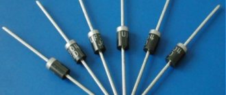
The PN crystal is commonly known as a junction diode . The word diode is an abbreviation for two electrodes, where di means two .
There are three possible offset for a PN connection:
- Equilibrium or zero bias - no external voltage is applied to the PN junction.
- Reverse bias - The positive terminal of the source is connected to n-type and the negative terminal of the source is connected to p-type.
- Forward bias - The negative terminal of the source is connected to n-type and the positive terminal of the source is connected to p-type.
Let's look at them one by one.
Equilibrium (zero displacement)
In a PN junction without an externally applied voltage, the equilibrium condition is achieved. Let's see how.
Depletion area
An n-type semiconductor has more free electrons than a p-type semiconductor. Because of this high concentration of electrons on the n-side, they repel each other.
Due to repulsion, free electrons spread (scatter) in all directions. Some of them cross the border between n and p. When a free electron enters the p region, it is attracted to the positive hole and recombines with it. When this happens, the hole disappears and the free electron becomes a valence electron.
When a free electron falls into a hole on the p-side, the p-side atom gains an extra electron. An atom that gains an extra electron has more electrons than protons, making it a negative ion.
Likewise, every free electron that leaves an n-side atom creates a hole in the n-side atom. An atom that loses an electron has more protons than electrons, making it a positive ion.
Thus, each time an electron crosses a junction and recombines with a hole, it creates a pair of ions. The following figure shows these ions on each side of the connection.
Each pair of positive and negative ions at the junction is called a dipole . Creating a dipole means that one free electron on the n-side and one hole on the p-side are removed from circulation. As the number of dipoles increases, the region near the transition becomes depleted of majority charge carriers. Therefore we call this uncharged region the depletion .
Barrier potential
Each dipole has an electric field between positive and negative ions. Whenever a free electron tries to enter the depletion region, this electric field pushes it back into the n region.
The electric field strength increases with each electron-hole recombination within the depletion region. Therefore, the electric field eventually stops the diffusion of electrons through the junction and equilibrium is achieved.
The electric field between ions is equivalent to a potential difference called the barrier potential . At room temperature, the barrier potential is approximately 0.3 V for germanium diodes and 0.7 V for silicon diodes.
Atoms and covalent bond
First, let's understand at the atomic level what and how it works. This will be a short introduction.
All matter is made up of molecules, and molecules in turn are made up of atoms. And every atom has protons, neutrons and electrons.
Protons and neutrons form a nucleus in which there are equal numbers of them.
The exception is hydrogen, which has only one proton in its nucleus, without a neutron.
There are orbits of electrons around the nucleus (by the way, it is now generally accepted that this is a cloud of electrons). Between them there are strong and weak forces, which are the basis of atoms. Further, we will not indicate protons and neutrons in the images for ease of perception.
Of course, one can delve further into the fact that there are mesons, quarks and other fundamental particles. And also that on the electronic shells of atoms, electrons are distributed in the form of a “gas” and they cannot be accurately detected, only with a certain degree of probability. However, this is not necessary to understand the operating principles of general digital electronics.
It is enough to simply accept the fact that there are atoms that have nuclei with a positive charge, and around this nucleus there are orbits with electrons.
Electrons and protons have opposite signs.
An electrically neutral atom has the same number of electrons and protons. All electrons are distributed over different levels. Those closest to the nucleus have two electrons, the next level has 4 electrons, and so on. But if for any reason an atom loses an electron, then that atom becomes a positive ion.
It lacks an electron in its outer electron orbital, which is called the valence level. It is easier to “take away” an electron from the valence level of an atom. And such electrons that are at the valence level are called valence electrons.
A positive ion (an atom that is deficient in electrons) will have a + sign because it is deficient in electrons and will attract or be attracted to a free electron (depending on the environment).
All atoms in molecules are connected to each other at the valence level, that is, using a covalent bond.
At the valence level, the bond between the nucleus and electrons is much smaller than at others, so atoms can form matter by combining with other atoms. This is how chemical reactions and atoms combine with each other.
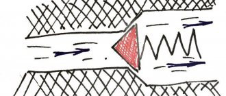
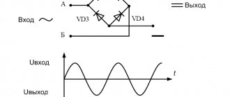
Forward offset
In forward bias, the p-type is connected to the positive terminal of the source and the n-type is connected to the negative terminal of the source. The following figure shows a forward bias diode.
If a battery is connected in this way, holes in the p-region and free electrons in the n-region are pushed towards the junction. If the battery voltage is less than the barrier potential (0.7 V), the free electrons do not have enough energy to pass through the depletion region. When they enter the depletion region, the ions push them back into the n-region. Because of this, current does not flow through the diode.
When the battery voltage exceeds the barrier potential (0.7 V), the free electrons have enough energy to pass through the depletion region and recombine with holes. In this way, they begin to neutralize the depletion area, reducing its width.
When a free electron recombines with a hole, it becomes a valence electron. As a valence electron, it continues to move to the left, passing from one hole to another until it reaches the left end of the diode.
When it leaves the left end of the diode, a new hole appears and the process begins again. Since billions of electrons are moving at the same time, we get a continuous current through the diode.
Application of pn junction
This is how a simple diode works, which consists of a pn junction. Simply put, a pn junction is a classic diode. And it can work both with direct connection and with reverse connection. In general, all modern digital technology consists of pn junctions.
Transistors, thyristors, microcircuits, logic elements, processors and much more are based on this.
Controlled avalanche breakdown
What happens if the voltage of the potential barrier is exceeded? For example, it is equal to 7 V. And in the diagram the source is 5 V. If we connect a source to 8 V, then an avalanche-like current will occur.
Minority charge carriers will take the majority ones with them. This process is partly controlled if we do not exceed the source voltage higher than the pn junction can withstand.
Electrical breakdown
If we increase the voltage even more, there will be an electrical breakdown. These phenomena are widely used in practice, for example, as stabilizers.
The current will not flow through the circuit until there is the voltage required to open the reverse biased pn junction.
And the electrical breakdown is controlled. Zener diodes (the so-called diodes that operate in this mode) are made specifically with wide pn junctions that operate for a long time under constant loads.
Thermal breakdown
But if the radio component is not initially designed for electrical breakdown, then it will quickly heat up and a thermal breakdown will occur. The holes and electrons will receive thermal energy, due to which the barrier will completely collapse. The junction heats up and cracks under the influence of temperature. This is an irreversible process.
In general, when equipment “burns out”, this is the phenomenon of thermal breakdown, that is, exceeding the permissible temperature.
And during soldering, thermal breakdown can also occur. It is enough to overheat the part a little and the pn junction will be destroyed.
Accordingly, if you pass a current through the diode that exceeds its capacity, then thermal breakdown will also occur. The same applies to power dissipation.
Reverse bias
Connecting p-type to the negative terminal of the battery and n-type to the positive terminal corresponds to reverse bias. The following figure shows a reverse biased diode.
The negative terminal of the battery attracts holes, and the positive terminal of the battery attracts free electrons. This causes holes and free electrons to flow out of the junction, leaving positive and negative ions behind. Consequently, the depletion area becomes wider.
The width of the depletion region is proportional to the reverse voltage. As the reverse voltage increases, the depletion region becomes wider. The depletion region stops growing when its potential difference is equal to the applied reverse voltage. When this happens, electrons and holes stop moving away from the connection.
How else is reverse inclusion used?
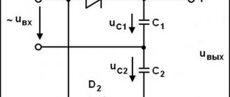
Also, reverse switching is very similar to a capacitor. Take a look at the diagram. These are two plates of a capacitor, in the middle of which there is a “dielectric”. And the electron-hole junction has a capacitance. And this is also used in practice. This is the name of a semiconductor capacitor.
In radio receivers, varicaps are used instead of interlinear capacitors. Varicaps are easy to set up. You just need to apply a reverse bias voltage of a certain value to increase or decrease the capacitance.
Of course, this is not the main application of a pn junction. Transition is used in different ways throughout digital technology.
Rectifiers, amplifiers, generators, processors, solar panels and much more. And what was described above about the operating principle of a pn junction is the operating principle of a conventional diode.
Reverse current
The reverse current in a diode consists of the minority carrier current and the surface leakage current. This reverse current is so small that you can't even notice it and it is considered almost zero.
Reverse saturation current
As is known, thermal energy continuously creates pairs of free electrons and holes. Suppose that thermal energy created a free electron and a hole inside the depletion region.
The depletion region pushes the newly created free electron into the n region, causing it to leave the right end of the diode. When it reaches the right end of the diode, it enters the outer wire and flows to the positive terminal of the battery.
On the other hand, the newly created hole is placed in the region p. This extra hole on the p side allows one electron from the negative terminal of the battery to enter the left end of the diode and fall into the hole.
Because thermal energy continuously creates electron-hole pairs within the depletion region, a small continuous current flows in the external circuit. This reverse current, caused by thermally generated minority carriers, is called saturation current . The name saturation means that increasing the reverse voltage will not increase the amount of thermally produced minority carriers.
Surface leakage current
A different current exists in a reverse biased diode. A small current flows across the surface of the crystal, known as surface leakage current .
The atoms on the top and bottom surfaces of the crystal have no neighbors. They have only six electrons in their valence orbital. This means that each surface atom has two holes. The following image shows these holes along the surface of the crystal.
Because of this, electrons pass through surface holes from the negative terminal of the battery to the positive terminal of the battery. Thus, a small reverse current flows along the surface.
Semiconductors and crystal lattice
Now we smoothly move on to semiconductors. Semiconductors such as silicon (Si) and germanium (Ge) each have 4 electrons at the covalent level.
Don't confuse flint and flint. Flint is a mineral and silicon is a chemical element that was discovered in 1810.
The peculiarity of semiconductors is that their atoms form pair bonds with each other.
Let's say there is a silicon atom. It has 4 electrons in its valence level. If you add 4 more silicon atoms to it, you get a crystal lattice. 4 atoms are connected to each other by their 4 electrons.
The picture shows the connection of atoms in a plane. In reality, it is naturally located not in one plane, but in space.
That is, each atom can form a stable bond with each other, 4 pieces on each side and plane.
The peculiarity of semiconductors is that this crystal lattice is very stable.
By the way, the conductivity of semiconductors strongly depends on external conditions (pressure, temperature, radiation, light). Much stronger than other materials. This is all due to the peculiarity of the crystal lattice, which will make it possible to make solar panels, sensors, cameras and much more.
So, atoms of semiconductors without impurities are electrically neutral.
And most importantly, they will still be connected to each other. A common covalent bond will allow them to exchange electrons with each other.
The conductivity of semiconductors under normal conditions is almost the same as that of dielectrics, that is, very low.
Breakdown
There is a limit to how much reverse voltage a diode will withstand before breakdown. If you keep increasing the reverse voltage, the diode will eventually reach its breakdown voltage.
Once the breakdown voltage is reached, a large number of minority carriers are generated in the depletion region due to the avalanche effect, and the diode begins to conduct strongly in the reverse direction.
Avalanche effect
As we know, there is a small carrier current in a reverse biased diode. When the reverse voltage increases, it causes the minority carriers to move faster.
These minority carriers, moving at high speed, collide with the crystal's atoms and knock out valence electrons, producing more free electrons. These new minority carriers attach to existing minority carriers and collide with other atoms, which knock out more electrons.
One free electron displaces one valence electron, resulting in two free electrons. These two free electrons then knock out two more electrons, resulting in four free electrons. Thus, the number of electrons increases exponentially : 1, 2, 4, 8...
This constant collision of atoms generates a large number of minority carriers, which produce a significant amount of reverse current in the diode. And this process continues until the reverse current becomes large enough to destroy the diode.
Barrier capacity.
As already noted, due to the diffusion of electrons and holes through the pn junction, uncompensated volumetric (spatial) charges of ionized impurity atoms arise in the transition region, which are fixed in the nodes of the crystal lattice of the semiconductor and therefore do not participate in the flow of electric current.
However, space charges create an electric field, which in turn most significantly affects the movement of free carriers of electricity, i.e., the process of current flow.
As the reverse voltage increases, the area of space charges (mainly due to the base) and the amount of charge in each layer (p and n) of the semiconductor increase. This increase occurs disproportionately: with a large modulus of reverse voltage, the charge increases with increasing modulus of voltage more slowly than with a small modulus of reverse voltage.
Let's give an explanatory illustration (Fig. 1.19), where we use the notation:
Q is the space charge in the n layer of the semiconductor;
u is the external voltage applied to the p-n junction.
Let us denote by f the function describing the dependence of Q on u. In accordance with the above
Q = f(u).
In the practice of mathematical modeling (and in manual calculations), it is convenient and therefore customary to use not this expression, but another, obtained from this as a result of differentiation. In practice, the so-called barrier capacitance of the C6ap-n-junction is widely used, and by definition, C6ap = | dQ/du | Let's draw graphs for Q (Fig. 1.20) and C bar (Fig. 1.21).
The phenomenon of emergence and change in the space charge of nonequilibrium carriers of electricity. Diffusion capacity.
If the voltage of an external voltage source biases the pn junction in the forward direction (u> 0), then injection (emission) begins - the entry of minority carriers of electricity into the semiconductor layer under consideration. In the case of an asymmetric pn junction (which usually happens in practice), the main role is played by injection from the emitter to the base.
We further assume that the transition is asymmetrical and that the emitter is layer p and the base is layer n. Then injection is the entry of holes into layer n. The consequence of injection is the appearance of holes in the base of a space charge.
It is known that in semiconductors the phenomenon of dielectric relaxation (Maxwell relaxation) occurs, which consists in the fact that the resulting space charge is almost instantly compensated by the charge of approaching free carriers of a different sign. This happens in about 10-12 s or 10-11 s.
In accordance with this, the charge of holes entering the base will be almost instantly neutralized by the same charge of electrons.
We use the following notation:
Q is the volume charge of nonequilibrium carriers in the base;
u is the external voltage applied to the p-n junction;
f is a function describing the dependence of Q on u.
Let's give an explanatory illustration (Fig. 1.22).
In accordance with the above, Q = f( u ) In practice, it is convenient and customary to use not this expression, but another, obtained from this as a result of differentiation. In this case, the concept of diffusion capacitance C diff of the pn junction is used, and by definition C diff = dQ / du The capacitance is called diffusion capacitance, since the charge Q under consideration underlies the diffusion of carriers in the base.
It is convenient and customary to describe Cdiff not as a function of voltage u, but as a function of current i of the pn junction.
The charge Q itself is directly proportional to the current i (Fig. 1.23, a). In turn, the current i depends exponentially on the voltage u (the corresponding expression is given above), therefore the derivative di / du is also directly proportional to the current (for an exponential function, the greater the value of the function, the greater the derivative). It follows that the capacitance Cdif is directly proportional to the current i (Fig. 1.23.6):
Cdif=i·τ/φт where φт is the temperature potential (defined above);
τ is the average time of flight (for a thin base), or lifetime (for a thick base).
The mean time of flight is the time during which the injected electrical carriers pass the base, and the lifetime is the time from the injection of the electrical carrier into the base until recombination.
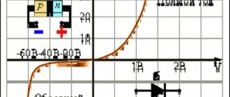
Diode IV characteristics
The following figure shows a basic diode circuit in which the diode is forward biased. Resistor RS is usually used to limit the forward current I F.
After connecting this circuit, if you measure the voltage and current of the diode for forward and reverse bias and plot it, you will get a graph that looks like this:
This graph is called current-voltage characteristic (IV) . This is the most important characteristic of a diode because it determines how much current flows through the diode for a given voltage.
A resistor is a linear device because its IV curve is a straight line. However, the diode is different. It is a non-linear device because its IV curve is not a straight line. This is due to the barrier potential.
Depending on the voltage applied to it, the diode will operate in one of three regions: forward bias, reverse bias, and breakdown.
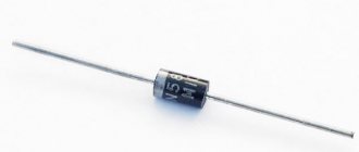
Rectifier diodes
Structurally, rectifier diodes are divided into planar and point diodes, and according to manufacturing technology into alloy, diffusion and epitaxial. Due to their large pn junction area, planar diodes are used to rectify large currents
.
Point diodes have a small transition area and, accordingly, are designed to rectify small currents
. To increase the avalanche breakdown voltage, rectifier columns are used, consisting of a series of diodes connected in series.
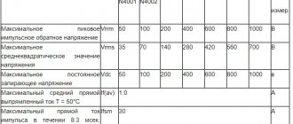
High power rectifier diodes are called power diodes
. The material for such diodes is usually silicon or gallium arsenide. Silicon alloy diodes are used to rectify alternating current with a frequency of up to 5 kHz. Silicon diffusion diodes can operate at higher frequencies, up to 100 kHz. Silicon epitaxial diodes with a metal substrate (with a Schottky barrier) can be used at frequencies up to 500 kHz. Gallium arsenide diodes are capable of operating in the frequency range up to several MHz.
Power diodes are usually characterized by a set of static and dynamic parameters. To static parameters
diodes include:
- voltage drop
Upr across the diode at a certain value of forward current; - reverse current
Irev at a certain value of reverse voltage; - average value of forward current
Ipr.av; - pulse reverse voltage
Urev.i.;
To dynamic parameters
diode include its time and frequency characteristics. These parameters include:
reverse voltage recovery time-
current rise time - maximum frequency
without reducing diode modes fmax.
Static parameters can be set using the current-voltage characteristic of the diode.
The diode reverse recovery time tres is the main parameter of rectifier diodes, characterizing their inertial properties. It is determined when the diode switches from a given forward current Ipr to a given reverse voltage Urev. During switching, the voltage across the diode becomes reversed. Due to the inertia of the diffusion process, the current in the diode does not stop instantly, but over time tout. Essentially, charge resorption occurs at the boundary of the pn junction (i.e., discharge of equivalent capacity). It follows from this that the power loss in the diode increases sharply when it is turned on, especially when turned off. Therefore, the losses in the diode
increase with increasing frequency of the rectified voltage.
When the temperature of the diode changes, its parameters change. The forward voltage on the diode and its reverse current depend most strongly on temperature. Approximately, we can assume that TKN (temperature coefficient of voltage) Upr = -2 mV/K, and the reverse current of the diode has a positive coefficient. So, with every 10 °C increase in temperature, the reverse current of germanium diodes increases by 2 times, and of silicon diodes by 2.5 times.
Forward bias area
When the diode voltage is less than the barrier potential, a small current flows through the diode. When the voltage across the diode exceeds the barrier potential, the current flowing through the diode increases rapidly.
The voltage at which the current begins to increase rapidly is called the forward voltage (VF) of the diode. This is also called turn-on voltage or knee voltage . Typically, a silicon diode has a VF of about 0.7 V, and a germanium diode has about 0.3 V.
Reverse bias region
The reverse bias region exists between zero current and breakdown.
In this region, a small reverse current flows through the diode. This reverse current is caused by thermally produced minority carriers. This reverse current is so small that you can't even notice it and it is considered almost zero.
Breakdown area
If you keep increasing the reverse voltage, you will eventually reach what is called diode breakdown voltage.
At this point, a process called avalanche breakdown , and the diode begins to conduct strongly in the opposite direction, breaking down.
The graph shows that the breakdown has a very sharp knee, followed by an almost vertical increase in current.