Voltage converters
High voltage converter for Geiger counter or photomultiplier
Converters for LDS
Boost converter DC(12V)->DC(xxV) with power up to 30W
Simple converter DC(12V)->DC(220V) up to 16 W
Boost converter DC(12V)->AC(220V, 50Gz) with power up to 100W
Boost converter DC(12V)->AC(220V,50Gz) 30 W
Boost converter on NE555 (12V->30V)
Converters based on KR1156EU5 (MC34063A)
Converter for charging a laptop from the car network (MC34063A)
Car voltage converter for laptop
Converter 1..5V -> 9..12V
Converter DC (1.5) -> DC (3.3/5) on KR1446PN1 (MAX756)
Converter 1.5V->5V
Unipolar to bipolar voltage converter (12V > +/-12V)
Unipolar to bipolar voltage converter (5V > +/-15V)
Converters for automobile UMZCH
Voltage-frequency converter
Replacement for "CRONE". Converter for MK ATtiny13A-SU
Replacement for "CRONE". Transistor converter
Replacing Krone with NCP1400ASN50T1
Drivers for isolated DC/DC converters
Bipolar voltage from unipolar to MK
Bipolar converter on BL8530 (0.6..1.5V -> +/-5V 10mA)
Low-power bipolar converter
Converter circuit 12DC/220AC (50Hz) “ASTRA”
Artificial midpoint in the power supply
Single-phase to three-phase voltage converters with frequency control
Artificial midpoint in the power supply
If you need to organize an artificial midpoint for devices with a consumption of up to 250 mA, you can use the proposed circuit. The input voltage can be in the range of 4...40V, which is divided in half by the TLE2426 precision divider; the BUF634T voltage follower increases the load capacity of the circuit.
Converter circuit 12DC/220AC (50Hz) “ASTRA”
Source: Yu. Bykovsky Restoration of the circuit diagram of the ASTRA voltage converter using a printed circuit board and its repair. — Radio, 2022, No. 11, p. 21-25 (No. 12, p. 18-20)
Simple UPS
The device proposed by the author simulates the operation of a UPS. Switching power from the network to a backup source is carried out using a relay. When powered from the mains, the battery recharging function is implemented. When powering the load with this converter, it must be taken into account that the frequency of the current at the converter output is 100 Hz.
In the original device, a homemade one was used as a step-up transformer T2, on a steel magnetic circuit Ш20х50. Winding I - 40 turns of wire with a diameter of 1.2 mm with a tap from the middle. Winding - II - 700 turns of wire, 0.35 mm in diameter. (When a voltage of 220 V is applied to winding II, there should be a voltage of approximately 6.5 V on winding I).
Transformer T1 with a power of approximately 25 VA and a voltage on the secondary winding of 15 V.
The S-150A battery over-discharge indicator can be replaced with LEDs.
Source: A.Eimov A simple uninterruptible power supply for a computer system unit. — Radio, No. 1, 2022, pp. 25-26
Converter for charging a laptop from the car network (MC34063A)
The converter is built on the MC34063A microcircuit according to a standard circuit. This device allows you to supply a voltage of 19V and a current of 0.6A (). Transistor VT1 can be used with almost any powerful one. From domestic ones, for example, the KT819 series. The BDX53C composite transistor has been practically tested. The transistor must be installed on a radiator; it is advisable to provide forced airflow. VD1 is almost any Schottky diode with a forward current of more than 1A and a reverse voltage of 40V or more.
Boost converter DC(12V)->AC(220V,50Gz) 30 W
About the details: Instead of KT805AM, you can use any powerful ones of a similar structure; in any case, they must be placed on heat sinks. The transformer can be made from any with a power of 30-50 W. All secondary windings are removed, and instead two are wound with PEV-2 1.28 wire, each with a number of turns corresponding to a transformation ratio of about 20 in relation to the 220V winding.
Source: S.Karoashchuk, V.Karlashchuk Converter for electric shaver. - Radio, 1989, No. 11, p. 69
Simple converter DC(12V)->AC(220V) up to 16 W
Converter designed for a rated operating voltage of 220 V DC and consuming power up to 16 W. Current consumption without load does not exceed 0.4 A, under load - 60 mA - 1.4 A. Efficiency - no worse than 0.75. The generation frequency of the converter at idle is about 850 Hz, under load it is about 650 Hz.
The converter is made using a push-pull transformer circuit on transistors VT1, VT2 and differs from other similar devices in that the emitter junctions of the transistors are connected in series, that is, one winding of the transformer T1 (winding III) is used to power the base circuits of both transistors. Diodes VD2, VD3 ensure the passage of control current, bypassing the emitter transition of the transistor, which is closed at one half cycle or another. The voltage drop across the open diode is quite sufficient to reliably close the transistor. At the same time, the diodes serve to protect the emitter junction of the transistors from breakdown. Resistor R1 limits the base current. Resistor R2 and capacitor C2 make up the startup circuit of the converter when it is turned on. The pulses taken from the secondary winding of transformer IV are rectified by a bridge assembled on diodes VD4 VD7 and filtered by capacitor C3. When the transistors switch, short-term voltage pulses with large amplitude occur, leading to an increase in the output voltage of the converter in idle mode. Load resistor R3 serves to reduce the output voltage at idle and discharges capacitor C3 when the converter power is turned off.
The KT837G silicon transistors used in the converter dissipate relatively little power and ensure its efficient operation. However, due to the large values of their static coefficient and limiting frequency, the converter is prone to switching to parasitic generation with an increased frequency (several tens of kilohertz). The most effective way to ensure stable operation is to connect inductor L1 in series to the power supply of the base circuits of the transistors.
Diode VD1 is used to protect the device in case of incorrect polarity of connection to the vehicle's on-board power supply or battery.
Transformer T1 is assembled on a magnetic core Ш8х16 with plates 0.08…0.15 mm thick made of steel E310, E320 or E330. You can use a magnetic core of a slightly larger standard size. Windings I and II contain 45 turns of wire PEV-1 0.47...0.51. III - 15 turns of wire PEV-1 0.2...0.35, IV - 900 turns of wire PEV-1 0.17...0.25. Winding IV is wound first, then I and II, and winding III last. All windings are laid turn to turn with insulation between layers. Windings I and II are wound into two wires simultaneously; identical parameters of these windings are necessary to reduce secondary voltage surges.
The device can use any transistors of the KT837 series with a saturation voltage between the collector and emitter of no more than 0.9 V, for example, with the indices G-K, P-F. It is possible to use germanium transistors of the P214, P215, P216, etc. series. In this case, inductor L1 can be eliminated.
Diodes VD2, VD3 - any of the KD105, KD208, KD209 series. Diodes VD4-VD7 (or a ready-made rectifier unit) must be designed for a reverse voltage of at least 800 V. Capacitor C1 - K50-6, C2 any, for example, KLS, KM. C3 - K50-12. Throttle L1 is serial - DM-0.2 or homemade.
Transistors are installed on heat sinks measuring 35x25x8 mm. Diode VD1 should also be equipped with a heat sink measuring 20x30x6 mm.
The criterion for the normal operation of the converter can be the current consumed at idle - if it is more than 0.3..0.4 A, it is necessary to slightly reduce the number of turns of winding III. The voltage at the output of the converter without load should be no more than 380 V, and when a load is connected - no less than 200 V.
When operating the device, the converter is first turned on, and then the load is turned on.
Source: A. Mezhlumyan Voltage converter for electric shaver. - Radio, 1988, No. 3, p. 48
Voltage-frequency converter
The nonlinearity of the converter with a coefficient of 4.2 kHz/V is no more than 3%. With an input voltage in the range of 0-5V, the frequency change is 0 - 21 kHz.
As DA1 you can use K140UD7, 555 series timer or KR1006VI1. The deviation of the values of resistors R1-R3, R5 is no more than 5%.
Converter 1.5V->5V
..on BL8530
The converter is built according to a typical circuit diagram for the BL8530 microcircuit. In standby mode, the converter consumes only 20-30 μA; for this it is necessary to use radioelements with low losses: tantalum capacitors, inductors with low active resistance and high quality factor at the conversion frequency of 350 kHz. Diode - pulsed low-power Schottky (type SS12-SS14). The choke can be wound on a ring with a diameter of 6.2 mm and a height of 3.2 mm. The winding contains 8 turns of PEV-2 0.4 wire.
All elements can be placed on the board shown below:
Note: The maximum power dissipation of the microcircuit depends on its size: SOT-89-3 - 0.3 W, SOT-23-3 - 0.15 W, SOT-23-5 - 0.15 W.
Source: I. Nechaev Voltage converters on the BL8530 microcircuit and devices based on them. - Radio, 2022, No. 7, p. 57-60
..on KR1446PN1 (MAX756)
The converter is designed to power a load with a voltage of 3.3 or 5 V with a current consumption of no more than 200 mA. The output voltage is set by jumper S1 (in the position indicated in the diagram - 3.3 V).
Jumper S2 is provided to implement control of turning on DA1.
..on YX8018
The YX8018 chip is used in lawn lights. On the basis, you can assemble a voltage converter from 0.8..1.5 V to 2.2..5 V and a load current of 6 mA. A detailed description is given in Zh.Radio, 2014, No. 5 p. 47.
Converters for automobile UMZCH
...circuitry of power supply units for automobile UMZCHs
The quality of the power supply of a car amplifier is no less important than the UMZCH itself. Here, even such little things as the cross-section of the supply wires play an important role. Typically, the level of transition attenuation of amplifiers with a common power supply is 40...55 dB for budget models, and 50...65 dB for more expensive ones. For amplifiers with separate power supplies, this figure exceeds 70 dB.
Supply voltage converters are divided into two groups - stabilized and unstabilized. Unstabilized ones are noticeably simpler and cheaper, but they have serious disadvantages: at signal peaks, the output voltage of the converter decreases, which leads to increased distortion. If you increase the power of the inverter, it will reduce the efficiency at low output power. Therefore, unstabilized converters are used, as a rule, in inexpensive amplifiers with a total channel power of no more than 100 ... 120 W. At higher amplifier output power, preference is given to stabilized converters.
Car amplifiers must use protection against load short circuits and overheating. In some cases, there is also load protection from DC voltage in the event of failure of the amplifier output stage.
In order to eliminate interference from the parasitic circuit (the length of the “ground” conductors in a car can reach 10 m or more), it is necessary to strive to ensure that the system has a single connection point with the body (body), but this condition cannot always be met. To reduce the level of interference, the common wire of the input circuits of the power supply and the common wire of its output circuits have complete galvanic isolation or are connected through a resistor R1 with a resistance of about 1 kOhm, as shown in Fig. 9 Depending on the location and method of installation of the amplifier, power and communication lines, in order to achieve a minimum level of interference, it may be necessary to directly connect the primary and secondary circuits.
The power supply for the Monacor HPB 150 amplifier is shown below in the figure:
The master oscillator is made using transistors VT106 and VT107 according to a symmetrical multivibrator circuit. The operation of the master oscillator is controlled by a key on transistor VT101. Transistors VT103, VT105 and VT102, VT104 are push-pull buffer cascades that improve the shape of the master oscillator pulses. The output stage is made of parallel-connected transistors VT111, VT113 and VT110. VT112. The matching emitter followers on VT108 and VT109 are powered by reduced voltage taken from part of the primary winding of the transformer. Diodes VD106 - VD111 limit the degree of saturation of the output transistors. To further speed up the closing of these transistors, diodes VD104, VD105 were introduced. Diodes VD102, VD103 ensure smooth startup of the converter. From a separate winding of the transformer, a voltage proportional to the output is supplied to the rectifier (diode VD113, capacitor C106). This voltage ensures active closing of the output transistors and helps stabilize the output voltage.
The disadvantage of bipolar transistors is the high saturation voltage at high current. At a current of 10...15 A, this voltage reaches 1 V, which significantly reduces the efficiency of the converter and its reliability. The conversion frequency cannot be raised above 25...30 kHz; as a result, the dimensions of the converter transformer and losses in it increase.
The use of field-effect transistors in the power supply (MOS Powered) increases reliability and efficiency. The conversion frequency in many blocks exceeds 100 kHz. The advent of specialized microcircuits containing a master oscillator and control circuits on a single chip has significantly simplified the design of power supplies.
A simplified circuit of an unstabilized power supply voltage converter for a four-channel Jensen amplifier is shown in the figure above.
The master oscillator is assembled on a KIA494P microcircuit (domestic analogue - KR1114EU4). The protection circuits are not shown in the diagram. In the output stage, in addition to the types of devices indicated in the diagram. You can use powerful field-effect transistors KP812V, KP850, IRF150, IRFP044 and IRFP054. 1N4118 diodes can be replaced with KD522B. The rectifier diodes KD2994, KD213 must be equipped with a heat sink. The design uses separate diode assemblies with a common anode and a common cathode, mounted through insulating pads together with the output transistors of the amplifier on a common heat sink.
The transformer can be wound on a ferrite ring K42x28x10 or K42x25x11 with a magnetic permeability of 2000. The primary winding is wound with a bundle of eight wires with a diameter of 1.2 mm. secondary - a bundle of four wires with a diameter of 1 mm. After winding, each of the bundles is divided into two equal parts, and the beginning of one half of the winding is connected to the end of the other. The primary winding contains 2×7 turns, the secondary winding contains 2×15 turns, evenly distributed around the ring.
Choke L1 is wound on a ferrite rod with a diameter of 16 mm and contains 10 turns of enameled wire with a diameter of 2 mm. Chokes L2, L3 are wound on ferrite rods with a diameter of 10 mm and contain 10 turns of wire with a diameter of 1 mm. The length of each rod is 20 mm.
A similar power supply circuit with minor changes is used in amplifiers with a total output power of up to 100... 120 W. The number of pairs of output transistors, transformer parameters and the design of protection circuits vary. In voltage converters of more powerful amplifiers, feedback on the output voltage is introduced and the number of output transistors is increased. To distribute the load evenly and reduce the influence of the scatter in the parameters of the transistors in the transformer, the currents of the powerful transistors are distributed over several primary windings; up to 20 powerful field-effect transistors can be used, 10 in each arm. The step-up transformer contains 5 primary windings, 4 transistors are connected to each of them (two in parallel in the arm). For better filtering of high-frequency interference, individual filter capacitors with a total capacity of 22,000 μF are installed near the transistors. The terminals of the transformer windings are connected directly to the transistors, without the use of printed conductors.
Source: A. Shikhatov Circuit design of automobile amplifiers. -Radio, 2001, No. 12, pp. 17-18
Converters based on KR1156EU5 (MC34063A)
Help on KR1156EU5
Datasheet MC34063 (pdf, English)
..increasing
The converter contains input and output filter capacitors C1, SZ, C4, storage choke L1, rectifier diode VD1. capacitor C2, which sets the operating frequency of the converter, inductor L2 for smoothing out ripples in the output voltage, resistors R1-R4.
Resistor R1 serves as a current sensor through the power switch. Voltage divider R2R3 sets the output voltage. It must be designed in such a way that, at the rated output voltage of the converter, a voltage of 1.25 V is supplied to the comparator input relative to pin 4 (Common) of the microcircuit.
Resistor R4 limits the collector current of the output switches (transistors) of the microcircuit. Deep saturation is dangerous because during the delay in opening the switch caused by it, the current in the inductor, continuing to increase, can reach a value that is unacceptable for the elements of the device. When calculating the value of resistor R4, another 7 mA is added to the required current value, which branches off in the internal circuit of the microcircuit.
The output voltage of the converter should not exceed 40 V. The maximum current through them should not be more than 1.5 A. To “power up” the microcircuit can be supplemented with a powerful bipolar transistor of any structure, as shown in the diagram below.
Below is a circuit design for constructing a 5 W boost converter with variations in output voltage from 45 to 190 V. Also, formulas are given for calculating converter elements for other output voltages.
In the magazine Radio 6/2009 pp. 51, 52 there is a diagram of a flashlight on a powerful LED using this microcircuit:
..downward
The converter operates similarly to that described above, but the output transistor of the microcircuit, connected in this case according to a circuit with a common collector, never enters saturation. This reduces the turn-off delay of the power switch, but increases the voltage drop across it, reducing the efficiency of the converter. A voltage greater than 40V cannot be supplied to the input of the step-down converter. Options for connecting “amplification” transistors are shown in the figure below.
..inverting
The peculiarity is that the DA1 microcircuit is powered by the sum of the input and output voltages, which should not exceed 40 V. “Amplification” is carried out in the same way as a step-down converter, however, the lower terminal of the resistor R5 in the circuit is connected not to the common wire , but to the emitter of the transistor VT3 .
..parts used and their calculation
Inductor L1 with an inductance of 170 μH for the converter according to the boost circuit is wound on three glued rings K 12x8x3 made of M4000NM ferrite with PESHO 0.5 wire, the winding consists of 59 turns. Before winding, each ring should be broken into two parts, filed with a file. Then a common 0.5 mm thick textolite gasket is inserted into one of the gaps and the entire package is glued together with epoxy glue. To maintain its shape, the bag is placed on a piece of organic glass, from which it can be easily separated after the glue has hardened. Before winding, the sharp edges of the rings should be carefully rounded. You can use the same ferrite rings with any permeability greater than 1000, since in the presence of a gap the inductance is practically independent of the magnetic permeability of the magnetic core material.
Inductor L1 with an inductance of 220 μH for the buck converter was wound in a similar way on three of the same rings, but the gluing gap was set to 0.25 mm, and the winding contained 55 turns of the same wire.
For inductor L1 of the inverting converter with an inductance of 88 μH, two of the same rings with a gap of 0.25 mm were used. number of turns - 35. wire - PEV-2 0.7.
Choke L2 in all converters is standard DM-2.4 with an inductance of 3 μH.
Oxide capacitors of converters - K50-35 or their imported analogues. Capacitors C2 are ceramic, for example, KM-5 or KM-6. Diode VD1 must be a Schottky diode; 1N5818, SR106, SR160 series KD268, KD269 and others with a voltage of at least 30 V are suitable. The converter will also work with conventional pulse diodes with a current of 1 A, but its efficiency will decrease.
Resistors R1 were made from high resistance wire with a diameter of 0.5 mm from a wirewound resistor. A piece of wire of the required length was folded into a snake and soldered into the holes of the printed circuit board.
The boost converter operating frequency is close to 15 kHz at 12 V input and rated load and 30 kHz for the other two.
Converters can work with chokes L1 of lower inductance, wound on single rings K 10x6x4.5 with a gap of 0.5 mm - 100 μH, 58 turns of PESHO 0.45 for boost, 130 μH, 66 turns of PESHO 0.38 for buck and 54 μH , 42 turns PESHO 0.5 for inverting. All of them turned out to be quite efficient, the efficiency and the range of permissible input voltages decreased slightly.
Source: S. Biryukov Converters based on the KR1156EU5 microcircuit. - Radio, 2000, No. 11, pp. 38, 42
Unipolar to bipolar voltage converter
In some cases, bipolar +/- 12V power may be required if unipolar 8-12V is available.
This circuit solution provides a load current of up to 50...60 mA, which is enough to power several op-amps.
Source: G.Shakhunov Refinement of the voltage converter. - Radio, 2001, No. 7, p. 39
Boost converter DC(12V)->AC(220V, 50Gz) with power up to 100W
The schematic diagram of a 100 W converter is shown in the figure. Circuit R1C1 was selected to obtain an output voltage frequency of about 50 Hz. Powerful composite transistors of the KT827 series (with indices A-B) connected in parallel are used as keys. Current equalizing resistors R9—R12 are made from pieces of copper wire with a diameter of 0.2 and a length of 100...200 mm. wound on MLT resistors with a power of 1 ... 2 W. It is also possible to use field-effect transistors connected in parallel, for example KP727A; in this case, current equalizing resistors are not required. Transformer T1 can be wound independently, but it is easier to use a unified filament transformer of the TN series with four filament windings with a voltage of 6.3 V each that is suitable in terms of power. They are connected in series, the free terminals are connected to the collectors of transistors VT1 - VT4, and the terminals of the second and third windings connected together are connected to the input of the voltage stabilizer DA2. To avoid overheating, transistors VT 1 - VT4 must be installed on heat sinks with an area of at least 600 cm2 and forced airflow must be used.
Source: A. Goreslavets Voltage converters on the KR1211EU1 microcircuit. - Radio, 2001, No. 5, pp. 42-43
Another circuit of a powerful converter is presented below (“Radio Television Electronics No. 6/98, p. 12-13):
The transformer is made on a magnetic core Ш36х36, windings W1′, W1 have 28 turns of PEL 2.1, W2 - 600 turns of PEL 0.59. First, the winding W2 is wound, and then with a double wire - W1′ and W1.
Boost converter DC(12V)->DC(xxV) with power up to 30W
The magnetic core of transformer T1 is ferrite (2000NM) armored or W-shaped with an average core cross-section of 0.4...1 cm2. The number of turns of the primary winding is determined at the rate of 1..1.5 turns per 1 V supply voltage, and the wire diameter is determined based on the current density of 3...5 A/mm2. For example, with an average primary winding current of 2 A, a wire with a diameter of 0.8 ... 1 mm should be used. The number of turns and diameter of the secondary winding wire are calculated in the same way. Capacitor C4 is selected based on the minimum heating of the transistors of the output switches (for a frequency of 40 kHz - 0.022...0.033 μF).
When using bipolar transistors, a supply voltage of 4...5 V to the microcircuit is sufficient, while the average current through the outputs of the microcircuit should not exceed 100 mA. Transistors should be selected with the highest possible operating frequency and maximum current transfer coefficient (for example, KT997A, KT9166A). To avoid overloading the outputs of the microcircuit, the capacitance of capacitors C2, SZ, which serve to force the opening and closing of transistors, should not exceed 0.1 μF. The maximum output power, in this case, will be 15W.
It is permissible to use field-effect transistors as output switches, for example, KP727A, KP921, Si9945, etc. (in this case, the converter power is 5...30 W). Their gates are connected directly to pins 4 and 6 of the DA1 microcircuit, the sources are connected to the common wire, and the drains are connected to the outer terminals of the primary winding of transformer T1, shunted by a capacitor. To fully open the field-effect transistors, the supply voltage of the microcircuit must be increased to approximately 8 V. To do this, connect a KS133A zener diode to pin 8 of the DA2 chip (anode to the common wire), and between pins 8 and 2 - a resistor with a resistance of 1 ... 1.2 kOhm.
When operating on an active load in the specified power range, output switch transistors usually do not require heat sinks, since converters of this type have a fairly high efficiency and, as a consequence, dissipate a small amount of heat.
Source: A. Goreslavets Voltage converters on the KR1211EU1 microcircuit. - Radio, 2001, No. 5, pp. 42-43
High voltage converter with a power of 0.5W
This converter can be used to power, for example, a Geiger counter or a photomultiplier.
Fig.1
The resistance of resistor R1 and the capacitance of capacitor C1 are selected from the condition of obtaining an oscillation frequency of the master oscillator equal to approximately 560 kHz, which corresponds to a conversion frequency of about 40 kHz.
The primary winding of transformer T1 is connected directly to the outputs of the microcircuit. The transformer magnetic core is W4x4 or W5x5 made of 2000NM ferrite. The primary winding must contain 24...30 turns of PEVT-2 0.1 wire. secondary (to obtain a voltage of about 400 V) - 1200... 1500 turns of PEVT-2 wire 0.04...0.06. The insulation between the windings is two layers of lavsan film 0.03...0.05 mm thick.
Diodes VD1-VD4 - any high-voltage diodes with a permissible reverse voltage of 800... 1000 V and an operating frequency of 30..50 kHz (for example, KD258G, KD258D, 2N4007).
Fig.2
T1 is made of two rings 16x10x4.5 mm from 3000NM ferrite. The rings are glued together and the sharp edges are rounded, then a layer of varnished cloth is wrapped. Winding III is wound first - 420 vit. PEV-2 0.07 mm, then a layer of insulation is wound. I wind windings I (8 volts) and II (3 volts) on top with any wire, distributing them evenly along the length of the magnetic circuit.
The generation frequency can be changed by changing the parameters R1 and C2. It should be taken into account that its increase leads to an increase in current consumption, and its decrease leads to a deterioration in the stability of the output current when the load changes.
Source:
- A. Goreslavets Voltage converters on the KR1211EU1 microcircuit. - Radio, 2001, No. 5, pp. 42-43
- Yu.Vinogradov Power supply of a gas-discharge counter. - Radio, 1989, No. 2, p. 61
Converter 1..5V -> 9..12V
A push-pull pulse generator is assembled using transistors VT1 and VT2. The positive feedback current flows through windings III and IV of transformer T1 and the load connected between the +12 V circuit and the common wire. Due to proportional current control of transistors, switching losses are significantly reduced and the efficiency of the converter is increased (can reach 82...85% at a load current of 1 A).
The role of diodes that rectify the output voltage is performed by the emitter junctions of the transistors. You can also obtain a negative voltage (in this case -4.2 V) by installing additional diodes VD1 and VD2. as shown in the figure with dashed lines. Here you will also need a filter capacitor, similar to C1, but connected in the opposite polarity.
The magnetic core of transformer T1 is a K 18x8x5 ring made of 2000NM1 ferrite. Windings I and II contain 6 turns each, and III and IV each contain 10 turns of insulated wire with a diameter of 0.5 mm. Each pair of windings is wound simultaneously into two wires.
The inverter is capable of operating when the input voltage is reduced to 1 V, which allows, for example, to obtain a voltage of 9 V from one galvanic cell with a voltage of 1.5 V. For a given input Uin and output Uout voltages and the number of turns w1 of windings I and II, the required number of turns windings III and IV (w2) are calculated with sufficient accuracy using the formula
w2=w1 (Uout-Uin+0.9)/(Uin-0.5)
Transistors should be selected based on the permissible values of the base current (it should not be less than the load current) and the emitter-base reverse voltage (it should be greater than twice the difference between the input and output voltages). In many cases, transistors of the KT208, KT209, KT501 series are suitable for operation in low-power converters. In this case, transformer T1 can be made on a ring magnetic core of smaller diameter.
Source: A. Chaplygin Simple voltage converter. - Radio, 2001, No. 11, p. 42.
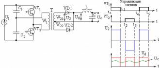
Boost converter on NE555 (12V->30V)
Timer DA1 (NE555) contains a pulse generator with a frequency of about 40 kHz (set by selecting R1, R2, C1). Next, the pulses arrive at V1, which operates in key mode. When it is open, energy accumulates in the inductor L1, and after the transistor closes, a voltage pulse appears in the coil several times higher than the supply voltage. The pulses are rectified by diode VD1 and charge capacitor C4. The output voltage is stabilized by zener diode VD2, ripples are smoothed out by capacitors C5-C6.
VT1 must have a collector-emitter voltage of at least 100V. The coil is wound with a wire with a diameter of 0.1 mm on an armored magnetic circuit to the specified inductance. You can use ready-made.
Source: Voltage converter. - Radio, 1998, No. 2, p. 63
Converters for LDS
The first device is described in [1].
The converter consists of a master oscillator and a single-ended power amplifier (Fig. 1). The generator is made on elements DD1.1-DD1.3 and allows you to adjust the duty cycle of the pulses with a variable resistor R1, which determines the brightness of the LDS. Buffer element DD1.4 is connected to the generator.
The signal from DD1.4 is fed to a power amplifier made of transistors VT1, VT2. The amplifier load is LDS (EL1), connected through step-up transformer T1. It is permissible to connect a lamp with both closed filament terminals (shown in the diagram) and open ones.
The converter is powered by a DC source with a voltage of 6... 12 V, capable of delivering current up to several amperes to the load (depending on the lamp power and set brightness). Power is supplied to the microcircuit through a parametric stabilizer, in which ballast resistor R4 and zener diode VD3 operate. At the minimum supply voltage, the stabilizer has practically no effect, but this does not affect the operation of the converter.
In addition to those indicated in the diagram, it is permissible to use transistors KT3117A, KT630B, KT603B (VT1), KT926A, KT903B (VT2), diodes of the KD503 series (VD1, VD2), zener diode D814A (VD3). Capacitor C1 - KT, KM, K10-17, the rest - K50-16, K52-1, K53-1. Variable resistor - any design (for example, SP2, SPZ), constant - OMLT-0.125. Lamp - power from 4 to 20 W.
The transformer is wound on an armored magnetic core made of 2000NM1 ferrite with an outer diameter of 30 mm. Winding I contains 35 turns of PEV-2 wire with a diameter of 0.45 mm, winding II contains 1000 turns of PEV-2 0.16. The windings are separated by several layers of varnished fabric. To increase reliability, winding II must be divided into several layers, laying varnished cloth between them. The magnetic circuit cups are assembled with a gap of 0.2 mm and tightened with a screw and nut made of non-magnetic material.
Setting up the converter begins with checking the master oscillator with the amplifier output stage turned off. An oscilloscope is connected to pin 11 of the microcircuit and the pulses shown in the upper diagram in Fig. are observed. 2. Then set the variable resistor slider to the left position according to the diagram (resistance is introduced). The duration of the pulses and their repetition period are measured. By selecting resistor R3, a pulse duration of approximately 20 μs is achieved, and by selecting resistor R2, a repetition period of approximately 50 μs is achieved. After this, moving the slider from one extreme position to another, one is convinced of the change in the repetition period of the pulses while their duration remains unchanged.
Next, the output stage is connected, the oscilloscope is connected to the collector of its transistor, and an ammeter with a scale of 2-3 A is placed in the power circuit. By moving the slider, they achieve “breakdown” (a sharp increase in brightness) of the lamp and control the range of changes in brightness and current consumption at different positions of the slider resistor. Observe the shape of the pulses on the collector of transistor VT2 - in Fig. 2 below, this shape was obtained when the converter was operated with an LB18 lamp. It may be necessary to more accurately select resistors R2, R7, and in some cases install a variable resistor of a different value in order to achieve the required limits for brightness changes and acceptable current consumption.
In the minimum brightness mode, which corresponds to a current of 250...400 mA depending on the supply voltage and lamp power, it is more convenient to start the generator, and therefore turn on the lamp, by pressing the SB1 button. Sometimes it’s a good idea to try changing the polarity of the lamp and check the reliability of its ignition in this mode.
The second option is described in [2] and involves using a ready-made transformer from an old TV
The converter is assembled according to a blocking generator circuit; it can also work with faulty lamps (with a burnt-out filament) with a power of up to 20 W. The circuit uses a TVS-110LA line transformer (from an old b/w TV). The latter is disassembled and the high-voltage winding and kenotron panel are removed. If the transformer “squeaks” during operation, then it is necessary to lubricate the ends of the core with glue. any powerful transistor, always on a radiator (you can use a different structure, but you will need to change the polarity of the power supply). The brightness of the glow is selected using resistor R1.
Winding diagram of the TVS-110 transformer
Source:
- V.Kobets Adjustable voltage converter for LDS. - Radio, 2000, No. 4, pp. 55-56
- A.Dmitriev LDS is powered by a battery. - radio, 2000, No. 3, p. 54
Generator using a telephone capsule
The generator shown in Fig. 9.3, uses the TK-67 telephone capsule as a load. This makes it possible to increase the amplitude of the generated pulses and thereby lower the lower limit of the start of generator operation by 200 mV.
By switching to a higher generation frequency, it is possible to continuously “pump” (convert) energy and significantly reduce the capacitance of capacitors.
Rice. 3. Circuit diagram of a low-voltage voltage converter generator using a telephone coil.
Converter architecture optimization
The selection of voltage converter components and assessment of their ultimate electrical characteristics should be based on the following initial data:
- converter output power;
- generator output voltage;
- mains voltage;
- specific design characteristics for a particular application.
Given the parameters of the generator and the requirements for the mains voltage, it is necessary to select an algorithm for the operation of the device. The multi-level structure of MVC allows you to use two modes of operation:
- Power regulation of cell inverters (max. power - 250 kW) regardless of the number of levels. Using this algorithm, the output power of the voltage converter is reduced when the cell is turned off.
- Regulation of the converter power (which is always the maximum - 1500 kW) regardless of the number of levels. In this case, the power of the cells must be selected with a margin in order to ensure the specified output characteristics when the cells are turned off.
From the point of view of economic efficiency of wind turbine operation, the first option is more preferable, which does not require the use of cells with excess power. Calculations of the operating modes of the converter were made based on the following initial data.
Nominal operating mode of the voltage converter:
- generator output power Vg - 1.5 MVA;
- generator output voltage (linear) Ug - 3000 V;
- generator current Ig - 288 A;
- DC bus voltage Vdc_conv - 4020 V;
- DC bus current Idc_conv - 373 A;
- input regulated voltage of the DC bus of the cell Vdc - 670 V;
- voltage on the DC link of the inverter Vdc_cell - 1000 V;
- input current DC inverter Idc_cell - 250 A;
- inverter output voltage (linear) Vond - 500 V;
- inverter phase current Iond - 288 A
Cell operating mode:
- cell output power Pout - 250 kVA;
- output voltage frequency fout - 60 Hz;
- cos φ: — 1;
- PWM inverter frequency fsw_o - 1.5 kHz;
- PWM chopper frequency fsw_b is 1 kHz.
The determination of power loss and overheating temperature (data shown in the table) was carried out using the thermal calculation program SemiSel [7].
Table