Key Mode
The operation of the transistor is probably one of the simplest (in terms of maintaining parameters) and at the same time very common of the transistor operating modes. At its core, the transistor most of the time is in only two states: cutoff and saturation. Below is a circuit diagram for switching on the transistor
To assemble a radio-electronic device, you can pre-make a DIY KIT kit using the link.
Using a transistor in switch mode
but before we begin to describe the operation of this circuit, it is necessary to declare a few simple rules under which the transistor operates
.
The rules are given for a pnp-type transistor
, but for an npn-type transistor they remain the same, but taking into account that
polarity
must be
reversed
:
What is an electronic key?
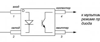
A key is, to simplify it, an ordinary switch. With its help, the electrical circuit is closed and opened. A bipolar transistor has three terminals:
- Collector.
- Emitter.
- Base.
Electronic switches are built on bipolar semiconductors - the design is simple and does not require a large number of elements. The switch is used to close and open a section of the circuit. This happens with the help of a control signal (which is generated by the microcontroller) supplied to the base of the transistor.
Load switching
Using simple circuits on transistor switches, you can switch currents in the range of 0.15... 14 A, voltages 50... 500 V. It all depends on the specific type of transistor. The key can switch a load of 5-7 kW using a control signal whose power does not exceed hundreds of milliwatts.
Instead of transistor switches, simple electromagnetic relays can be used. They have the advantage that they do not heat up during operation. But the frequency of on and off cycles is limited, so they cannot be used in inverters or switching power supplies to create a sine wave. But in general, the principle of operation of a switch on a semiconductor transistor and an electromagnetic relay is the same.
Electromagnetic relay
A relay is an electromagnet that controls a group of contacts. An analogy can be drawn with a conventional push-button switch. Only in the case of a relay, the force is taken not from the hand, but from the magnetic field that is located around the excitation coil. The contacts can switch a very large load - it all depends on the type of electromagnetic relay. These devices have become very widespread in automotive technology - with their help, all powerful consumers of electricity are turned on.
This allows you to divide all the electrical equipment of the car into a power part and a control part. The current consumption of the relay excitation winding is very small. And the power contacts are coated with precious or semi-precious metals, which eliminates the possibility of an arc. Transistor switch circuits for 12 volts can be used instead of relays. At the same time, the functionality of the device improves - the switching on is silent, the contacts do not click.
Example of work
Let's take a closer look at how a simple transistor switch functions. The switched signal is transmitted from one input and removed from the other output. To lock the key, a voltage is applied to the transistor gate that exceeds the source and drain values by an amount greater than 2-3 V. But care should be taken not to go beyond the permissible range. When the key is closed, its resistance is relatively high - more than 10 ohms. This value is obtained due to the fact that the reverse bias current of the pn junction also influences. In the same state, the capacitance between the switched signal circuit and the control electrode fluctuates in the range of 3-30 pF. Now let's open the transistor switch. The diagram and practice will show that then the voltage of the control electrode will approach zero, and strongly depends on the load resistance and the switched voltage characteristic. This is due to a whole system of interactions between the gate, drain and source of the transistor. This creates certain problems for operating in chopper mode.
As a solution to this problem, various circuits have been developed that provide stabilization of the voltage that flows between the channel and the gate. Moreover, due to its physical properties, even a diode can be used in this capacity. To do this, it should be included in the forward direction of the blocking voltage. If the necessary situation is created, the diode will close and the pn junction will open. So that when the switching voltage changes, it remains open and the resistance of its channel does not change, a high-resistance resistor can be connected between the source and input of the switch. And the presence of a capacitor will significantly speed up the process of recharging the containers.
Electromagnetic relay terminals
Typically, electromagnetic relays have 5 terminals:
- Two contacts for control. The excitation winding is connected to them.
- Three contacts intended for switching. One common contact that is normally closed and normally open with the others.
Depending on which switching scheme is used, groups of contacts are used. The field-effect transistor switch has 3-4 contacts, but it functions in approximately the same way.
How does an electromagnetic relay work?
The operating principle of an electromagnetic relay is quite simple:
- The winding is connected to the power supply through a button.
- The power contacts of the relay are connected to the consumer's power supply circuit break.
- When you press the button, power is supplied to the winding, the plate is attracted and the group of contacts is closed.
- Current is supplied to the consumer.
Transistor switches work in approximately the same way - only a group of contacts is missing. Their functions are performed by a semiconductor crystal.
Transistor conductivity
One of the operating modes of the transistor is key. Essentially, it acts as a switch. There is no point in touching on the circuits of the amplifier stages; they do not relate to this mode of operation. Semiconductor triodes are used in all types of devices - in automotive technology, in everyday life, in industry. All bipolar transistors can have this type of conductivity:
- PNP.
- NPN.
The first type includes semiconductors made on the basis of germanium. These elements became widespread more than half a century ago. A little later, silicon, which has reverse conductivity - npn, began to be used as an active element.
The operating principle of the devices is the same; they differ only in the polarity of the supply voltage, as well as in certain parameters. Silicon semiconductors are currently more popular; they have almost completely replaced germanium semiconductors. And most devices, including transistor switches, are made on bipolar silicon elements with npn conductivity.
Calculation of a switch for a transistor
Let's add a payload in the form of an LED to the circuit. Resistor R_k remains in place, it will limit the current through the load and ensure the required operating mode:
Suppose that to turn on the LED you need to apply a voltage of 3V (U_d) to it. In this case, the diode will consume a current equal to 50 mA (I_d). Let's set the transistor parameters (in real circuits, these values are taken from the documentation for the transistor used):
- Current gain h_{21e} = 100…500 (the range is always specified, not a specific value)
- The voltage drop across the base-emitter junction required to open this junction: U_{be} = 0.6 medspace V.
- Saturation voltage: U_{ke medspace us} = 0.1 medspace V.
We take specific values for calculations, but in practice everything is somewhat different. As you remember, the parameters of transistors depend on many factors, in particular on the operating mode, as well as on temperature. And the ambient temperature, of course, can change. It is not so easy to determine clear values from the characteristics, so you need to try to ensure a small margin. For example, when calculating, it is better to take the current gain equal to the minimum of the values given in the datasheet. After all, if the coefficient in reality is higher, then this will not disrupt the operation of the circuit; of course, the efficiency will be lower, but nevertheless the circuit will work. And if we take the maximum value of h_{21e}, then under certain conditions it may turn out that the real value turned out to be less, and it is no longer sufficient to ensure the required operating mode of the transistor.
So, let's return to the example. The input data for the calculation, among other things, are the voltages of the sources. In this case:
- E_{in} = 3.3medspace Q. I chose a typical value that is found in practice when developing circuits on microcontrollers. In this example, this voltage is turned on and off by switch S_1.
- E_{out} = 9medspace B.
First of all, we need to calculate the resistance of the resistor in the collector circuit. The voltages and currents of the output circuit in the on state are related as follows:
U_{ke medspace us} + U_{R_k} + U_d = E_{out}
In this case, according to Ohm's law:
U_{R_к} = I_к R_к
And we have a given current, since we know how much current the load (in this case, a diode) consumes when it is on. Then:
U_{R_k} = I_d R_kU_{ke medspace us} + I_d R_k + U_d = E_{out}
So, in this formula we know everything except the resistance, which needs to be determined:
R_к = frac{E_{out} medspace — medspace U_д medspace — medspace U_{ке medspace us}}{I_д} enspace= frac{9 medspace B medspace — medspace 3 medspace B medspace — medspace 0.1 medspace B}{0.05 medspace A} medspaceapprox 118 medspace Ohm.
It will be interesting➡ PNP transistor
We select an available resistance value from the standard range of ratings and get R_{к} = 120medspace Ohm. Moreover, it is important to choose a larger value. This is due to the fact that if we take a value slightly larger than calculated, then the current through the load will be slightly less. This will not lead to any malfunctions. If you take a smaller resistance value, this will lead to the fact that the current and voltage at the load will exceed the specified ones, which is worse
Let's recalculate the collector current value for the selected resistance value:
I_к = frac{U_{R_к}}{R_к} medspace = frac{9 medspace V medspace — medspace 3 medspace V medspace — medspace 0.1 medspace V}{120 medspace Ohm} medspaceapproxmedspace 49.17 medspace mA
It's time to determine the base current; for this we use the minimum gain value:
I_b = frac{I_к}{h_{21е}} = frac{49.17 medspace mA}{100} = 491.7 medspace μA
And the voltage drop across resistor R_b:
U_{R_b} = E_{in} medspace — medspace 0.6 medspace B = 3.3 medspace B medspace — medspace 0.6 medspace B = 2.7 medspace B
Now we can easily determine the resistance value:
R_b = frac{U_{R_b}}{I_b}medspace = frac{2.7 medspace V}{491.7 medspace μA} approx 5.49 medspace KOhm
Again we turn to a number of acceptable denominations. But now we need to choose a value less than the calculated one. If the resistor resistance is greater than the calculated value, then the base current will, on the contrary, be less. And this can lead to the fact that the transistor does not open completely, and when it is on, most of the voltage will drop across the transistor (U_{ke}), which, of course, is undesirable.
Therefore, we select a value of 5.1 KOhm for the base resistor. And this stage of calculation was the last! Let's recap, our calculated denominations were:
- R_{b} = 5.1medspace KOhm
- R_{k} = 120medspace Ohm
By the way, in a transistor switch circuit, a resistor is usually added between the base and emitter, with a nominal value of, for example, 10 KOhm. It is needed to tighten the base when there is no signal at the input. In our example, when S1 is open, the input simply hangs in the air. And under the influence of interference, the transistor will randomly open and close. Therefore, a pull-up resistor is added so that in the absence of an input signal, the base potential is equal to the emitter potential. In this case, the transistor will be guaranteed to be closed.
Today we went through the classical scheme, which I try to adhere to, that is, from theory to practice. I hope that the material will be useful, and if you have any questions, write in the comments, I will be happy to help!
Transistor in switch mode
A transistor in switch mode performs the same functions as an electromagnetic relay or switch. The control current flows as follows:
- From the microcontroller via the base-emitter junction.
- In this case, the collector-emitter channel opens.
- Through the collector-emitter channel you can pass a current whose value is hundreds of times greater than the base one.
The peculiarity of transistor switches is that the switching frequency is much higher than that of a relay. A semiconductor crystal is capable of making thousands of transitions from an open state to a closed state and back in one second. Thus, the switching speed of the simplest bipolar transistors is about 1 million times per second. For this reason, transistors are used in inverters to create a sine wave.
Let's summarize:
- Look at the picture below.
- Select a bias scheme.
- Select RK and IE for your application. The values of RK and IE should usually set the collector voltage VK to 1/2 of Vsupply.
- Calculate the base resistor RB to obtain the required emitter current.
- If necessary, recalculate the emitter current IE for standard resistor values.
- For a voltage divider bias circuit, first calculate the emitter bias and then determine R1 and R2.
- For AC amplifiers: a bypass capacitor in parallel with RE improves the AC voltage gain. Select XC≤0.10RE for the lowest frequency.
Formulas for calculating displacement (in brief)
Original article:
- Biasing Calculations
Transistor operating principle
The element works exactly the same as in power amplifier mode. Essentially, a small control current is applied to the input, which is amplified several hundred times due to the fact that the resistance between the emitter and collector changes. Moreover, this resistance depends on the amount of current flowing between the emitter and the base.
Depending on the type of transistor, the pinout changes. Therefore, if you need to determine the pins of an element, you need to consult a reference book or datasheet. If it is not possible to refer to the literature, you can use reference books to determine conclusions. There is also a peculiarity of transistors - they may not open completely. Relays, for example, can be in two states - closed and open. But for a transistor, the resistance of the emitter-collector channel can vary within wide limits.
Bipolar transistors. For dummies
Preface
Since the topic of transistors is very, very extensive, there will be two articles devoted to them: separately on bipolar and separately on field-effect transistors.
A transistor, like a diode, is based on the pn junction phenomenon. Those who wish can refresh their memory of the physics of the processes occurring in it here or here. The necessary explanations have been given, let's get to the point.
Transistors. Definition and history
A transistor
is an electronic semiconductor device in which the current in a circuit of two electrodes is controlled by a third electrode.
(transistors.ru)
Field-effect transistors were the first to be invented (1928), and bipolar transistors appeared in 1947 at Bell Labs.
And it was, without exaggeration, a revolution in electronics. Very quickly, transistors replaced vacuum tubes in various electronic devices. In this regard, the reliability of such devices has increased and their size has decreased significantly. And to this day, no matter how “sophisticated” the microcircuit is, it still contains many transistors (as well as diodes, capacitors, resistors, etc.). Only very small ones.
By the way, initially “transistors” were resistors whose resistance could be changed using the amount of applied voltage. If we ignore the physics of processes, then a modern transistor can also be represented as a resistance that depends on the signal supplied to it.
What is the difference between field-effect and bipolar transistors? The answer lies in their very names. In a bipolar transistor, charge transfer also
electrons
and
holes (“encore” - twice).
And in field (also known as unipolar) there are either
electrons
or
holes.
Also, these types of transistors differ in application areas. Bipolar ones are used mainly in analog technology, and field ones - in digital technology.
And finally: the main area of application of any transistors
— strengthening of a weak signal due to an additional power source.
Bipolar transistor. Principle of operation. Main characteristics
A bipolar transistor consists of three regions: emitter, base and collector, each of which is supplied with voltage.
Depending on the type of conductivity of these areas, npn and pnp transistors are distinguished. Typically the collector area is wider than the emitter area. The base is made of a lightly doped semiconductor (which is why it has high resistance) and is made very thin. Since the emitter-base contact area is significantly smaller than the base-collector contact area, it is impossible to swap the emitter and collector by changing the connection polarity. Thus, the transistor is an asymmetrical device. Before considering the physics of how a transistor operates, let's outline the general problem.
It is as follows: a strong current flows between the emitter and the collector ( collector current
), and between the emitter and the base there is a weak control current (
base current
). The collector current will change depending on the change in base current. Why? Let's consider the pn junctions of the transistor. There are two of them: emitter-base (EB) and base-collector (BC). In the active mode of operation of the transistor, the first of them is connected with forward bias, and the second with reverse bias. What happens at the pn junctions? For greater certainty, we will consider an NPN transistor. For pnp everything is similar, only the word “electrons” needs to be replaced with “holes”.
Since the EB junction is open, electrons easily “run across” to the base. There they partially recombine with holes, but b o
Most of them, due to the small thickness of the base and its low doping, manage to reach the base-collector transition.
Which, as we remember, is reverse biased. And since electrons in the base are minority charge carriers, the electric field of the transition helps them overcome it. Thus, the collector current is only slightly less than the emitter current. Now watch your hands. If you increase the base current, the EB junction will open more, and more electrons will be able to slip between the emitter and collector. And since the collector current is initially greater than the base current, this change will be very, very noticeable. Thus, the weak signal received at the base will be amplified
. Once again, a large change in collector current is a proportional reflection of a small change in base current.
I remember that the principle of operation of a bipolar transistor was explained to my classmate using the example of a water tap. The water in it is the collector current, and the base control current is how much we turn the knob. A small force (control action) is enough to increase the flow of water from the tap.
In addition to the processes considered, a number of other phenomena can occur at the pn junctions of the transistor. For example, with a strong increase in voltage at the base-collector junction, avalanche charge multiplication may begin due to impact ionization. And coupled with the tunnel effect, this will give first an electrical breakdown, and then (with increasing current) a thermal breakdown. However, thermal breakdown in a transistor can occur without electrical breakdown (i.e., without increasing the collector voltage to breakdown voltage). One excessive current through the collector will be enough for this.
Another phenomenon is due to the fact that when the voltages on the collector and emitter junctions change, their thickness changes. And if the base is too thin, then a closing effect may occur (the so-called “puncture” of the base) - a connection between the collector junction and the emitter junction. In this case, the base region disappears and the transistor stops working normally.
The collector current of the transistor in the normal active mode of operation of the transistor is greater than the base current by a certain number of times. This number is called the current gain
and is one of the main parameters of the transistor.
It is designated h21
.
If the transistor is turned on without load on the collector, then at a constant collector-emitter voltage, the ratio of the collector current to the base current will give a static current gain
. It can be equal to tens or hundreds of units, but it is worth considering the fact that in real circuits this coefficient is smaller due to the fact that when the load is turned on, the collector current naturally decreases.
The second important parameter is the input resistance of the transistor
. According to Ohm's law, it is the ratio of the voltage between the base and emitter to the control current of the base. The larger it is, the lower the base current and the higher the gain.
The third parameter of a bipolar transistor is voltage gain
. It is equal to the ratio of the amplitude or effective values of the output (emitter-collector) and input (base-emitter) alternating voltages. Since the first value is usually very large (units and tens of volts), and the second is very small (tenths of volts), this coefficient can reach tens of thousands of units. It is worth noting that each base control signal has its own voltage gain.
Transistors also have a frequency response
, which characterizes the transistor’s ability to amplify a signal whose frequency approaches the cut-off amplification frequency.
The fact is that as the frequency of the input signal increases, the gain decreases. This is due to the fact that the time of occurrence of the main physical processes (the time of movement of carriers from the emitter to the collector, the charge and discharge of capacitive barrier junctions) becomes commensurate with the period of change of the input signal. Those. the transistor simply does not have time to react to changes in the input signal and at some point simply stops amplifying it. The frequency at which this happens is called the cutoff frequency
.
Also, the parameters of the bipolar transistor are:
- reverse current collector-emitter
- on time
- reverse collector current
- maximum permissible current
The symbols for npn and pnp transistors differ only in the direction of the arrow indicating the emitter. It shows how current flows in a given transistor.
Operating modes of a bipolar transistor
The option discussed above represents the normal active mode of operation of the transistor. However, there are several more combinations of open/closed pn junctions, each of which represents a separate mode of operation of the transistor.
- Inverse active mode
. Here the BC transition is open, but on the contrary, the EB is closed. The amplification properties in this mode, of course, are worse than ever, so transistors are used very rarely in this mode. - Saturation mode
. Both crossings are open. Accordingly, the main charge carriers of the collector and emitter “run” to the base, where they actively recombine with its main carriers. Due to the resulting excess of charge carriers, the resistance of the base and pn junctions decreases. Therefore, a circuit containing a transistor in saturation mode can be considered short-circuited, and this radio element itself can be represented as an equipotential point. - Cut-off mode
. Both transitions of the transistor are closed, i.e. the current of the main charge carriers between the emitter and collector stops. Flows of minority charge carriers create only small and uncontrollable thermal transition currents. Due to the poverty of the base and transitions with charge carriers, their resistance increases greatly. Therefore, it is often believed that a transistor operating in cutoff mode represents an open circuit. - Barrier mode
In this mode, the base is directly or through low resistance closed to the collector. A resistor is also included in the collector or emitter circuit, which sets the current through the transistor. This creates the equivalent of a diode circuit with a resistor in series. This mode is very useful, as it allows the circuit to operate at almost any frequency, over a wide temperature range and is undemanding to the parameters of the transistors.
Switching circuits for bipolar transistors
Since the transistor has three contacts, in general, power must be supplied to it from two sources, which together produce four outputs. Therefore, one of the transistor contacts has to be supplied with a voltage of the same sign from both sources. And depending on what kind of contact it is, there are three circuits for connecting bipolar transistors: with a common emitter (CE), a common collector (OC) and a common base (CB). Each of them has both advantages and disadvantages. The choice between them is made depending on which parameters are important to us and which can be sacrificed.
Connection circuit with common emitter
This circuit provides the greatest gain in voltage and current (and hence in power - up to tens of thousands of units), and therefore is the most common.
Here the emitter-base junction is switched on directly, and the base-collector junction is switched on reversely. And since both the base and the collector are supplied with voltage of the same sign, the circuit can be powered from one source. In this circuit, the phase of the output AC voltage changes relative to the phase of the input AC voltage by 180 degrees. But in addition to all the goodies, the OE scheme also has a significant drawback. It lies in the fact that an increase in frequency and temperature leads to a significant deterioration in the amplification properties of the transistor. Thus, if the transistor must operate at high frequencies, then it is better to use a different switching circuit. For example, with a common base.
Connection diagram with a common base
This circuit does not provide significant signal amplification, but is good at high frequencies, since it allows more full use of the frequency response of the transistor.
If the same transistor is connected first according to a circuit with a common emitter, and then with a common base, then in the second case there will be a significant increase in its cutoff frequency of amplification. Since with such a connection the input impedance is low and the output impedance is not very high, transistor cascades assembled according to the OB circuit are used in antenna amplifiers, where the characteristic impedance of the cables usually does not exceed 100 Ohms. In a common-base circuit, the signal phase does not invert, and the noise level at high frequencies is reduced. But, as already mentioned, its current gain is always slightly less than unity. True, the voltage gain here is the same as in a circuit with a common emitter. The disadvantages of a common base circuit also include the need to use two power supplies.
Connection diagram with a common collector
The peculiarity of this circuit is that the input voltage is completely transmitted back to the input, i.e. the negative feedback is very strong.
Let me remind you that negative feedback is such feedback in which the output signal is fed back to the input, thereby reducing the level of the input signal. Thus, automatic adjustment occurs when the input signal parameters accidentally change
The current gain is almost the same as in the common emitter circuit. But the voltage gain is small (the main drawback of this circuit). It approaches unity, but is always less than it. Thus, the power gain is equal to only a few tens of units.
In a common collector circuit, there is no phase shift between the input and output voltage. Since the voltage gain is close to unity, the output voltage matches the input voltage in phase and amplitude, i.e., repeats it. That is why such a circuit is called an emitter follower. Emitter - because the output voltage is removed from the emitter relative to the common wire.
This connection is used to match transistor stages or when the input signal source has a high input impedance (for example, a piezoelectric pickup or a condenser microphone).
Two words about cascades
It happens that you need to increase the output power (i.e. increase the collector current).
In this case, parallel connection of the required number of transistors is used. Naturally, they should be approximately the same in characteristics. But it must be remembered that the maximum total collector current should not exceed 1.6-1.7 of the maximum collector current of any of the cascade transistors. However (thanks to wrewolf for the note), this is not recommended in the case of bipolar transistors. Because two transistors, even of the same type, are at least slightly different from each other. Accordingly, when connected in parallel, currents of different magnitudes will flow through them. To equalize these currents, balanced resistors are installed in the emitter circuits of the transistors. The value of their resistance is calculated so that the voltage drop across them in the operating current range is at least 0.7 V. It is clear that this leads to a significant deterioration in the efficiency of the circuit. There may also be a need for a transistor with good sensitivity and at the same time good gain. In such cases, a cascade of a sensitive but low-power transistor (VT1 in the figure) is used, which controls the power supply of a more powerful fellow (VT2 in the figure).
Other applications of bipolar transistors
Transistors can be used not only in signal amplification circuits. For example, due to the fact that they can operate in saturation and cutoff modes, they are used as electronic keys. It is also possible to use transistors in signal generator circuits. If they operate in the key mode, then a rectangular signal will be generated, and if in the amplification mode, then a signal of arbitrary shape, depending on the control action.
Marking
Since the article has already grown to an indecently large volume, at this point I will simply give two good links, which describe in detail the main marking systems for semiconductor devices (including transistors): https://kazus.ru/guide/transistors/mark_all .html and .xls file (35 kb).
List of sources:
https://ru.wikipedia.org https://www.physics.ru https://radiocon-net.narod.ru https://radio.cybernet.name https://dvo.sut.ru
Helpful comments:
https://habrahabr.ru/blogs/easyelectronics/133136/#comment_4419173
An example of transistor operation in switch mode
Gain is one of the main characteristics of a transistor. It is this parameter that shows how many times the current flowing through the emitter-collector channel is higher than the base one. Let's say the coefficient is 100 (this parameter is designated h21E). This means that if a current of 1 mA (base current) is supplied to the control circuit, then at the collector-emitter junction it will be 100 mA. Consequently, the incoming current (signal) was amplified.
During operation, the transistor heats up, so it needs passive or active cooling - radiators and coolers. But heating occurs only when the collector-emitter passage does not open completely. In this case, a lot of power is dissipated - it needs to be put somewhere, you have to “sacrifice” the efficiency and release it in the form of heat. Heating will be minimal only in cases where the transistor is closed or fully open.
Fixed Base Current Bias Circuit
The simplest bias circuit uses a base bias resistor between the base and the base battery Vbias. Using an existing Vpit source instead of a new bias source is very convenient. An example of this bias circuit is shown in the audio amplifier stage of a detector receiver in the RF Circuits section of Chapter 9. Note the resistor between the base and battery terminal. A similar diagram is shown in the figure below.
Write the equation of Kirchhoff's voltage law for a circuit that includes a battery, RB and the voltage drop VBE across the transistor junction in the figure below. Please note that we use the notation Voffset, although in fact it is Vpit. If the coefficient β is large, we can make the approximation that IK = IE. For silicon transistors VBE ≅ 0.7 V.
Fixed Base Current Bias Circuit
\[V_{offset} - I_B R_B - V_{BE} = 0\]
\[V_{offset} - V_{BE} = I_B R_B\]
\[I_B = { V_{offset} - V_{BE} \over R_B }\]
\[I_E = (\beta + 1)I_B \approx \beta I_B\]
\[I_E = { V_{displacement} - V_{BE} \over R_B / \beta }\]
The β coefficient of small-signal transistors is typically in the range of 100–300. Assuming we have a β=100 transistor, what value of base bias resistor would be required to achieve 1mA emitter current?
Solving the IE equation to determine RB and substituting the values of β, Voffset, VBE and IE will give the result 930 kOhm. The closest standard value is 910 kOhm.
\(\beta = 100 \qquad V_{offset} = 10 V \qquad I_K \approx I_E = 1 mA \)
\[R_B = { V_{offset} - V_{BE} \over I_E / \beta } = { 10 - 0.7 \over 1 mA / 100 } = 930 kOhm \]
What will be the emitter current with a 910 kOhm resistor? What happens to the emitter current if we replace the transistor with a random one with β=300?
\(\beta = 100 \qquad V_{offset} = 10 V \qquad R_B = 910 kOhm \qquad V_{BE} = 0.7 V\)
\[I_E = { V_{offset} - V_{BE} \over R_B / \beta } = { 10 - 0.7 \over 910 kOhm / 100 } = 1.02 mA \]
\(\beta = 300\)
\[I_E = { 10 - 0.7 \over 910 kOhm / 300 } = 3.07 mA \]
When using a standard 910 kOhm resistor, the emitter current will change slightly. However, when β changes from 100 to 300, the emitter current triples. This is unacceptable for a power amplifier if we expect the collector voltage to vary from near Vsupply to near ground. However, for low level signals from microvolts to about a volt, the bias point can be centered at β equal to the square root of (100 300), which is equal to 173. The bias point will still drift over a significant range. However, low level signals will not be clipped.
A fixed base current bias circuit is inherently unsuitable for the large emitter currents used in power amplifiers. The emitter current in a bias circuit with a fixed base current is not temperature stable. Temperature runaway is the result of high emitter current, which causes an increase in temperature, which causes an increase in emitter current, which will further increase the temperature.
Saturation mode
All transistors have a certain input current threshold. Once this value is reached, the gain ceases to play a big role. In this case, the output current does not change at all. The voltage at the base-emitter contacts can be higher than between the collector and emitter. This is a saturation state, the transistor opens completely. The key mode means that the transistor operates in two modes - either it is completely open or closed. When the control current supply is completely cut off, the transistor closes and stops passing current.
Auto bias circuit (with commutator feedback)
Bias changes due to temperature and beta can be reduced by moving the bias resistor terminal from the voltage source Vbias to the collector of the transistor, as shown in the figure below. If the emitter current increases, the voltage drop across RK will increase, which will reduce the voltage VK, which will reduce the IB supplied back to the base. This in turn will reduce the emitter current, correcting the initial increase.
Let's write the equation of Kirchhoff's voltage law for a circuit that includes a battery, RK, RB and voltage drop VBE. Let's replace IК≅IE and IB≅IE/β. Solving for IE gives the IE formula for the automatic bias circuit with commutator feedback. Solving for RB gives the RB formula for the automatic bias circuit with collector feedback.
Automatic commutator feedback bias circuit
\[I_K = \beta I_B \qquad I_K \approx I_E \qquad I_E \approx \beta I_B \]
\[V_{pit} - I_К R_К - I_Б R_Б -V_{БЭ} = 0\]
\[V_{pit} - I_E R_K - (I_E/ \beta) R_B -V_{BE} = 0\]
\[V_{pit} -V_{BE} = I_E R_K + (I_E/ \beta) R_B\]
\[V_{pit} -V_{BE} = I_E (( R_B / \beta) + R_K)\]
\[I_E = {V_{pit} -V_{BE} \over R_B / \beta + R_K }\]
\[R_B = \beta \left[ {V_{pit} -V_{BE} \over I_E } - R_K \right] \]
Let's find the required bias resistor for feedback with the collector for an emitter current of 1 mA, a collector load resistor of 4.7 kOhm and a transistor with β = 100. Let's find the collector voltage VK. It should be approximately halfway between Vpit and the housing.
\(\beta = 100 \qquad V_{pit} = 10 V \qquad I_K \approx I_E = 1 mA \qquad R_K = 4.7 kOhm \)
\[R_B = \beta \left[ {V_{pit} - V_{BE} \over I_E } - R_K \right] = 100 \left[ {10 - 0.7 \over 1 mA } - 4.7 kOhm \ right] = 460 kOhm \]
\[ V_K = V_{pit} - I_K R_K = 10 - (1 mA) (4.7 kOhm) = 5.3 V \]
The closest standard value to a 460k resistor for automatic biasing with collector feedback is 470k. Let's find the emitter current IE for a 470 kOhm resistor. Let's recalculate the emitter current for transistors with β=100 and β=300.
\(\beta = 100 \qquad V_{supply} = 10 V \qquad R_K = 4.7 kOhm \qquad R_B = 470 kOhm \)
\[I_E = {V_{pit} -V_{BE} \over R_B / \beta + R_K } = {10 -0.7 \over 470 kOhm / 100 + 4.7 kOhm } = 0.989 mA \]
\(\beta = 300\)
\[I_E = {V_{pit} -V_{BE} \over R_B / \beta + R_K } = {10 -0.7 \over 470 kOhm / 300 + 4.7 kOhm } = 1.48 mA \]
We see that as beta changes from 100 to 300, the emitter current increases from 0.989 mA to 1.48 mA. This is an improvement over the previous fixed base current bias design, where the emitter current increased from 1.02 mA to 3.07 mA. When changing beta, collector feedback bias is twice as stable as fixed base bias.
Practical designs
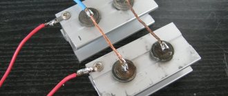
There are a lot of practical schemes for using transistors in switch mode. They are often used to turn LEDs on and off to create special effects. The operating principle of transistor switches allows not only to make “toys”, but also to implement complex control circuits. But in designs it is imperative to use resistors to limit the current (they are installed between the source of the control signal and the base of the transistor). But the source of the signal can be anything - a sensor, a push-button switch, a microcontroller, etc.
Working with microcontrollers
When calculating a transistor switch, you need to take into account all the operating features of the element. In order for the control system on the microcontroller to work, amplification stages on transistors are used. The problem is that the output signal from the controller is very weak, it is not enough to turn on the power to the winding of the electromagnetic relay (or open the transition of a very powerful power switch). It is better to use a bipolar transistor switch to control the MOSFET element.
Simple designs are used, consisting of the following elements:
- Bipolar transistor.
- Resistor to limit input current.
- Semiconductor diode.
- Electromagnetic relay.
- Power supply 12 volts.
The diode is installed in parallel with the relay winding; it is necessary in order to prevent breakdown of the transistor by a pulse with a high EMF, which appears when the winding is turned off.
The control signal is generated by the microcontroller, goes to the base of the transistor and is amplified. In this case, power is supplied to the winding of the electromagnetic relay - the collector-emitter channel opens. When the power contacts are closed, the load is turned on. The transistor switch is controlled in a fully automatic mode - practically no human intervention is required. The main thing is to correctly program the microcontroller and connect sensors, buttons, and actuators to it.
4.1. ???
If the load of the OE key is a sufficiently large capacity, then the key has low performance.
Let's assume that the transistor in the key circuit turns off instantly.
Rice. 3.1.a: Key diagram after switching (previously it was saturated) |
The output voltage is the voltage across the capacitor.
The previously discharged capacity begins to charge with current.
The duration of the front is determined by the charging time of the capacitance, that is. Since it is several kOhms, the duration of the falling edge turns out to be unacceptably long.
| For example: ; . Then . |
To improve the parameters of the key, it is built according to the structural diagram:
Rice. 3.1.b: Key structure diagram |
In this circuit, there is a low-resistance circuit for charging.
The principle of operation of a composite key is as follows.
When a positive pulse arrives at the input, the OE switch closes and the OK switch opens. The load capacity is quickly discharged through a saturated OE switch. The output voltage is close to zero.
At the end of the positive pulse, the OE key opens and the OK key closes. Now the load capacity is charged through the saturated OK switch. Since the saturation current of the transistor is high, the capacitance is charged quickly.
Rice. 3.1.c: Schematic diagram of a composite key |
A star key is assembled on transistor VT1, which represents a combination of OE and OK keys. The signal at the collector has a polarity opposite to the polarity of the input signal, that is, the collector circuit VT1 acts as an inverter. The emitter circuit VT1 does not invert the signal.
VT2 - OK key;
VT3 - OE key.
1) If transistor VT1 is locked, then
.
Since, transistor VT3 is also locked.
The voltage at the collector VT1 is:
and close to the supply voltage.
Therefore, transistor VT2 is open and the load capacitance in steady state is charged to voltage
,
where , is the voltage drop across the emitter junction of the open transistor VT2 and across the open diode VD1.
2) If the transistor is saturated, then
and transistor VT3 is also in saturation mode. In this case, VT2 must be locked. To do this, it is necessary that the voltage at its base be less than or equal to the voltage at the emitter or
From the last relationship it is clear that in the absence of a diode in the circuit, the condition for turning off transistor VT2 is not satisfied.
In this state of the key, the capacitance is discharged through the saturated transistor VT3 and the voltage across it (low level).
During the transition process, due to the delay in turning off the transistors, some transistors (both VT2 and VT3) are open for some time. This results in an inrush of current drawn by the key from the power supply. To limit this current, a small resistance is introduced into the collector circuit of transistor VT2
Often, transistor VT2 with diode VD is replaced with a composite transistor VT2′, VT2".
Rice. 3.1.d: Composite transistor VT2′, VT2" |
The principle of operation of the circuit does not change. The function of the bias diode VD here is performed by the emitter junction of transistor VT2.”
Use of transistors in designs
You need to study all the requirements for semiconductors that you are going to use in the design. If you plan to control the winding of an electromagnetic relay, then you need to pay attention to its power. If it is high, then it is unlikely to be possible to use miniature transistors like KT315: they will not be able to provide the current necessary to power the winding. Therefore, it is recommended to use high-power field-effect transistors or assemblies in power engineering. Their input current is very small, but the gain is large.
You should not use powerful relays to switch weak loads: this is unreasonable. Be sure to use high-quality power sources, try to choose the voltage so that the relay operates in normal mode. If the voltage is too low, the contacts will not attract and switching will not occur: the magnitude of the magnetic field will be small. But if you use a source with a high voltage, the winding will begin to heat up and may even fail.
Be sure to use low and medium power transistors as buffers when working with microcontrollers if you need to turn on powerful loads. It is better to use MOSFET elements as power devices. The connection diagram to the microcontroller is the same as that of the bipolar element, but there are slight differences. The operation of a transistor switch using MOSFET transistors occurs in the same way as with bipolar ones: the transition resistance can change smoothly, transferring the element from an open state to a closed state and back.
3.1. Residual parameters of a closed transistor
a) When the value of the blocking voltage at the emitter junction changes, that is, when the cutoff depth () changes, the base current does not change and remains equal. This equality is called the current cutoff criterion.
b) Both in the deep cutoff mode and at the cutoff boundary, the emitter current is .
The equivalent circuit of the key in cut-off mode can be represented as:
| Rice. 2.1.a: Equivalent circuit of a key in cut-off mode |
Switch output voltage
c) From the diagram it is clear that the voltage applied to the emitter, control junction depends on the residual base current;
.
In its turn .
To maintain the cutoff mode when changing from and resistances, it is necessary to fulfill the following condition:
.
Otherwise, despite the negative polarity of the control signal, the transistor will switch to active mode.
d) In transistor switches, it is necessary to use transistors with low reverse transition currents.
Note:
Integrated circuits do not use negative control signals to turn off transistors because digital circuits are single-supply powered. The open state of the key does not correspond to the cut-off mode, but to the active mode at low collector current. This has a beneficial effect on reducing the duration of transient processes.
|
The transistor turn-off threshold is a conditional value. The more open, the more can be selected. Usually accepted.