Photo of a digital chip
A microcircuit is an electronic device or part of it capable of performing a particular task. If it were necessary to solve such a problem, which is solved by many microcircuits, using discrete elements, using transistors, then the device, instead of a small rectangle measuring 1 centimeter by 5 centimeters, would occupy an entire cabinet and would be much less reliable. But this is what computers looked like half a hundred years ago!
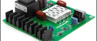
Electronic control cabinet - photo
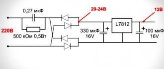
Of course, for a microcircuit to work, it is not enough to simply supply power to it; you also need a so-called “body kit,” that is, those auxiliary parts on the board with which the microcircuit can perform its function.
Chip body kit - drawing
In the figure above, the microcircuit itself is highlighted in red; all other parts are its “body kit”. Very often, microcircuits heat up during their operation; these can be microcircuits for stabilizers, amplifiers, microprocessors and other devices. In this case, to prevent the microcircuit from burning out, it must be attached to a radiator. Microcircuits that must heat up during operation are designed immediately with a special heat sink plate - a surface usually located on the back side of the microcircuit, which should fit tightly to the radiator.
Photo of the microcircuit from the side attached to the radiator
But in the connection, even with a carefully polished radiator and plate, there will still be microscopic gaps, as a result of which heat from the microcircuit will be less efficiently transferred to the radiator.
In order to fill these gaps, heat-conducting paste is used. The same one that we apply to the computer processor before fixing the radiator on top of it. One of the most widely used pastes is KPT-8 .
Paste KPT-8
Amplifiers on microcircuits can be soldered in literally 1-2 evenings, and they begin to work immediately, without the need for complex setup and highly qualified tuners. Separately, I would like to say about car amplifier microcircuits; sometimes there are literally 4-5 parts from a body kit. To assemble such an amplifier, with some care, you don’t even need a printed circuit board (although it is desirable) and you can assemble everything using a surface-mounted installation, directly on the pins of the microcircuit.
Amplifier assembled by wall mounting
True, after assembly, it is better to immediately place such an amplifier in a housing, because such a design is unreliable, and in the event of an accidental short circuit of the wires, the microcircuit can easily be burned. Therefore, I recommend that all beginners spend a little more time making a printed circuit board.
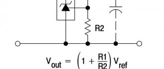
Adjustable on-chip voltage regulator
Regulated power supplies based on stabilizer chips are even easier to manufacture than similar ones based on transistors. Look how many parts a simple LM317 microcircuit replaces:
Microcircuits on printed circuit boards in electronic devices can be soldered either directly to print tracks or placed in special sockets.
Socket for deep chip - photo
The difference is that in the first case, in order to replace the microcircuit, we will have to desolder it first. And in the second case, when we put the microcircuit in the socket, we just need to remove the microcircuit from the socket, and it can be easily replaced with another one. A typical example of replacing a microprocessor in a computer.
PC Socket-478 CPU
Also, for example, if you are assembling a device on a microcontroller on a printed circuit board, and have not provided for in-circuit programming, you can, if you soldered into the board not the chip itself, but the socket into which it is inserted, then the chip can be removed and connected to a special programmer board .
View of the programmer board with sockets
Such boards already have sockets soldered into different microcontroller housings for programming.
Story
The invention of microcircuits began with the study of the properties of thin oxide films, which manifest themselves in the effect of poor electrical conductivity at low electrical voltages.
The problem was that where the two metals touched, there was no electrical contact or it was polar. Deep studies of this phenomenon led to the discovery of diodes and later transistors and integrated circuits. In 1958, two scientists living in completely different places invented an almost identical integrated circuit model. One of them, Jack Kilby, worked for Texas Instruments, the other, Robert Noyce, was one of the founders of the small semiconductor manufacturing company Fairchild Semiconductor. Both were united by the question: “How to fit a maximum of components into a minimum of space?” Transistors, resistors, capacitors and other parts were placed separately on boards at that time, and scientists decided to try to combine them on one monolithic chip made of semiconductor material. Only Kilby used germanium, and Noyce preferred silicon. In 1959, they separately received patents for their inventions - a confrontation between the two companies began, which ended with a peace treaty and the creation of a joint license for the production of chips. After Fairchild Semiconductor Corporation made integrated circuits commercially available in 1961, they were immediately used in the production of calculators and computers instead of individual transistors, allowing for significant reduction in size and increased performance.
The first Soviet semiconductor microcircuit was created in 1961 at the Taganrog Radio Engineering Institute, in the laboratory of L. N. Kolesov.
The first semiconductor integrated circuit in the USSR was developed (created) on the basis of planar technology developed at the beginning of 1960 at NII-35 (then renamed the Pulsar Research Institute) by a team that was later transferred to NIIME (Mikron). The creation of the first domestic silicon integrated circuit was concentrated on the development and production with military acceptance of the TC-100 series of integrated silicon circuits (37 elements - the equivalent of the circuit complexity of a flip-flop, an analogue of the American IC series SN-51 from Texas Instruments). Prototype samples and production samples of silicon integrated circuits for reproduction were obtained from the USA. The work was carried out by NII-35 (director Trutko) and the Fryazino plant (director Kolmogorov) under a defense order for use in an autonomous altimeter of a ballistic missile guidance system. The development included six standard integrated silicon planar circuits of the TS-100 series and, with the organization of pilot production, took three years at NII-35 (from 1962 to 1965). It took another two years to develop factory production with military acceptance in Fryazino (1967).
Integrated Circuit Design Idea
The idea behind a chip was to take the complete circuit, with all its many electronic components and connections, and then recreate it in microscopic form on the surface of a piece of silicon. Thanks to this idea, all sorts of “microelectronic” gadgets emerged that are now taken for granted:
- digital clock,
- pocket calculators,
- space rockets,
- satellite navigation and much more.
Integrated circuits revolutionized electronics and computing during the 1960s and 1970s. Gradually, integrated circuits were modernized, which was accompanied by an increase in the scale of integration of electronic components while maintaining (and even reducing) small overall dimensions:
- Small Scale Integration (SSI)
- Medium Scale Integration (MSI)
- Large Scale Integration (LSI)
- Very Large Scale Integration (VLSI)
- Ultra Large Scale Integration (ULSI)
Manufacturing technologies
Types of logic
The main element of analog microcircuits are transistors (bipolar or field-effect). The difference in transistor manufacturing technology significantly affects the characteristics of microcircuits. Therefore, the manufacturing technology is often indicated in the description of the microcircuit, thereby emphasizing the general characteristics of the properties and capabilities of the microcircuit. Modern technologies combine bipolar and field-effect transistor technologies to achieve improved performance of microcircuits.
- Microcircuits based on unipolar (field-effect) transistors are the most economical (in terms of current consumption): MOS logic (metal-oxide-semiconductor logic) - microcircuits are formed from n
-MOS or
p
-MOS type field-effect transistors; - CMOS logic (complementary MOS logic) - each logic element of the microcircuit consists of a pair of complementary (complementary) field-effect transistors ( n
-MOS and
p
-MOS).
- RTL - resistor-transistor logic (obsolete, replaced by TTL);
- BiCMOS
Using the same type of transistors, microcircuits can be created using different methodologies, for example, static or dynamic.
CMOS and TTL (TTLS) technologies are the most common logic chips. Where it is necessary to save current consumption, CMOS technology is used, where speed is more important and saving power consumption is not required, TTL technology is used. The weak point of CMOS microcircuits is their vulnerability to static electricity - just touch the output of the microcircuit with your hand, and its integrity is no longer guaranteed. With the development of TTL and CMOS technologies, the parameters of microcircuits are getting closer and, as a result, for example, the 1564 series of microcircuits are made using CMOS technology, and the functionality and placement in the case are similar to TTL technology.
Microcircuits manufactured using ESL technology are the fastest, but also the most energy-consuming, and were used in the production of computer equipment in cases where the most important parameter was calculation speed. In the USSR, the most productive computers of the ES106x type were manufactured on ESL microcircuits. Nowadays this technology is rarely used.
Technological process
Main article: Process technology in the electronics industry
See also: Moore's Law
In the manufacture of microcircuits, the method of photolithography (projection, contact, etc.) is used, in which the circuit is formed on a substrate (usually silicon) obtained by cutting single crystals of silicon with diamond disks into thin wafers. Due to the small linear dimensions of microcircuit elements, the use of visible light and even near ultraviolet radiation for illumination was abandoned.
As a characteristic of the technological process of producing microcircuits, the minimum controlled dimensions of the photorepeater topology (contact windows in silicon oxide, gate width in transistors, etc.) and, as a consequence, the dimensions of transistors (and other elements) on the chip are indicated. This parameter, however, is interdependent with a number of other production capabilities: the purity of the resulting silicon, the characteristics of the injectors, photolithography methods, etching and sputtering methods.
In the 1970s, the minimum controlled size of commercially produced microcircuits was 2-8 microns, in the 1980s it was reduced to 0.5-2 microns[11].
In the 1990s, due to a new round of the “platform war,” experimental methods began to be introduced into production and rapidly improved: in the early 1990s, processors (for example, early Pentium
and
Pentium Pro
) were manufactured using 0.5-0.6 micron technology (500-600 nm), then the technology reached 250-350 nm.
The following processors ( Pentium
II,
K
6-2+,
Athlon
) were already made using 180 nm technology. In 2002-2004, 90 nm technological processes were mastered (Winchester AMD 64, Prescott Pentium 4)[11].
The following processors were fabricated using UV light (ArF excimer laser, wavelength 193 nm). On average, industry leaders introduced new technological processes according to the ITRS plan every 2 years, which ensured a doubling of the number of transistors per unit area: 45 nm (2007), 32 nm (2009), 22 nm (2011)[12][13], production 14nm started in 2014[14], development of 10nm processes is expected around 2022.
In 2015, estimates emerged that the introduction of new technological processes would slow down[15].
Quality control
To control the quality of integrated circuits, so-called test structures are widely used.
What are Logic Integrated Circuits (ICs)
Essentially, this is a microelectronic device that is based on a crystal of arbitrary complexity, which is made on a semiconductor film or wafer. It is placed in a non-separable case (although it can do without it, but only when it is part of a microassembly). The first integrated circuit was patented in 1968. This was a kind of breakthrough in the industry, although the provided device did not very much correspond to modern ideas in its parameters. Integrated circuits are mostly manufactured for surface mounting. Often, IC is understood as just one crystal or film. The most widespread is the integrated circuit on a silicon wafer. It so happens that its use in industry has a number of advantages, for example, the efficiency of signal transmission.
What is an integrated circuit
An integrated circuit is a miniature electronic unit containing in a common housing transistors, diodes, resistors and other active and passive elements, the number of which can reach several tens of thousands.
One microcircuit can replace an entire unit of a radio receiver, an electronic computer (computer) and an electronic machine. The “mechanism” of a digital wristwatch, for example, is just one larger chip.
According to their functional purpose, integrated circuits are divided into two main groups: analog, or linear-pulse, and logical, or digital, microcircuits.
Analog microcircuits are intended for amplification, generation and conversion of electrical oscillations of different frequencies, for example, for receivers, amplifiers, and logical ones - for use in automation devices, in devices with digital timekeeping, in computers.
This workshop is devoted to familiarization with the device, operating principle and possible application of the simplest analog and logical integrated circuits.
Design Levels
- Physical - methods of implementing one transistor (or a small group) in the form of doped zones on a crystal.
- Electrical - circuit diagram (transistors, capacitors, resistors, etc.).
- Logical - logical circuit (logical inverters, OR-NOT, AND-NOT elements, etc.).
- Circuit and system level - circuit and system design (flip-flops, comparators, encoders, decoders, ALUs, etc.).
- Topological - topological photomasks for production.
- Program level (for microcontrollers and microprocessors) - assembler instructions for the programmer.
Currently, most integrated circuits are developed using CAD systems, which make it possible to automate and significantly speed up the process of obtaining topological photomasks.
How are integrated circuits created?
How to make a memory chip or computer processor? The manufacturing process begins with the chemical element silicon, which is chemically treated (alloyed) to impart different electrical properties.
MEMORY CHIP
A modern design of an integrated circuit (one of many forms) installed on the electronic board of the device. This is far from the most advanced option, but only one of many
Traditionally, materials of two categories are used for electronics needs:
- Conductors.
- Insulators.
But technically, everything is more complicated, especially when it comes to certain elements in the middle of the periodic table (groups 14 and 15), in particular silicon and germanium. What is noteworthy is that insulating materials can become conductors if a certain amount of impurities is added to these materials. A process known as alloying.
Production.
Manufacturing an integrated circuit can take up to two months because certain areas of the semiconductor must be precisely doped. In a process called crystal growing, or crystal pulling, a cylindrical slab of high-purity silicon is first produced. From this cylinder, plates with a thickness of, for example, 0.5 mm are cut. The wafer is eventually cut into hundreds of small pieces called chips, each of which is transformed into an integrated circuit through the process described below.
The chip processing process begins with the production of masks for each layer of the IC. A large-scale stencil is made, shaped like a square with an area of approx. 0.1 m2. A set of such masks contains all the components of the IC: diffusion levels, interconnect levels, etc. The entire resulting structure is photographically reduced to the size of a crystal and reproduced layer by layer on a glass plate. A thin layer of silicon dioxide is grown on the surface of the silicon wafer. Each plate is coated with a light-sensitive material (photoresist) and exposed to light transmitted through masks. Unexposed areas of the photosensitive coating are removed with a solvent, and with the help of another chemical reagent that dissolves silicon dioxide, the latter is etched from those areas where it is no longer protected by the photosensitive coating. Variations of this basic process technology are used in the fabrication of two main types of transistor structures: bipolar and field-effect (MOS).
Main types of modern microcircuits
It is important to understand that progress does not stand still: every year the list of main types of microcircuits undergoes significant changes, in addition, their range is expanding.
The types of microcircuits are different, depending on the main evaluation criteria.
By purpose:
1. Digital. Necessary for processing a special signal expressed in digital code. They have a significant number of advantages over other types: lower costs for electricity consumption, in addition, they have greater resistance to interference.
Digital microcircuits are often used in various computers, such as automation systems, electronic computers and many others.
2. Analog. Designed for processing and converting continuously incoming signals. Analog chips have high performance. Often used in such popular devices as:
Video recorders.
Televisions.
Audio frequency converters.
In various voltage stabilizers.
In sensors.
Operational amplifiers.
3. Analog-digital. They are a true hybrid of the two microcircuits presented above. They are very popular due to their increased performance indicators; in addition, they combine the positive characteristics of two types of microcircuits at once. They are used to create most modern technology, such as:
Modulators and demodulators.
Switches.
Frequency generators and restorers.
By type of construction:
1. Film. These are microcircuits for the manufacture of which a special technique is used. In addition, all connecting elements are a special film layer. There are certain divisions into two types: thin-film and thick-film, differing in the thickness of the film layer.
2. Semiconductor chips are not used very often; they are made using plastic (usually epoxy resin) with special wire or tape leads that ensure the performance of the device.
3. Hybrid. More complex devices, for the manufacture of which not only popular films and substrates are used, but also less common attachment materials (for example, various crystals).
By body type:
1. Cabinet. With this type of design, the microcircuit is placed in a special case (the material from which it is made can be chosen by the manufacturer). This type is not particularly popular in everyday life. Most often, the microcircuit is placed in a housing in order to avoid breakage or deformation of individual parts during transportation.
Packaged microcircuits are used to transport large quantities of goods. In any other case, it is cheaper for the manufacturer to produce unpackaged microcircuits.
2. Unpackaged microcircuits. Most often, it is the open-frame models that are used. The microcircuit does not fit into the case; in this case, for protection, all parts are filled with special paint or compound. This is what allows you to protect the crystal from damage or any other negative environmental influences.
Such designs are produced specifically for installation in a hybrid circuit or preliminary microassembly.
When choosing a microcircuit, you should take into account all the advantages and disadvantages of the main types. Certain technical devices require certain microcircuits; in order to select the required model, it is necessary to obtain professional advice from specialists in this field. In this case, the device you choose will last a long time.
Classification
Degree of integration
Depending on the degree of integration, the following names of integrated circuits are used:
- small integrated circuit (MIC) - up to 100 elements per chip
- medium integrated circuit (SIS) - up to 1000 elements per chip
- large integrated circuit (LSI) - up to 10 thousand elements per chip
- ultra-large-scale integrated circuit (VLSI) - more than 10 thousand elements per chip
Previously, now outdated names were also used: ultra-large-scale integrated circuit (ULSI) - from 1-10 million to 1 billion elements in a chip [9] [10] and, sometimes, giga-large-scale integrated circuit (GBIC) - more than 1 billion elements in a crystal. Currently, in the 2010s, the names “UBIS” and “GBIS” are practically not used, and all microcircuits with more than 10 thousand elements are classified as VLSI.
Manufacturing technology
Hybrid microassembly STK403-090, removed from the case
- Semiconductor chip - all elements and inter-element connections are made on one semiconductor crystal (for example, silicon, germanium, gallium arsenide).
For more details see Planar technology
- Film integrated circuit - all elements and inter-element connections are made in the form of films: thick film integrated circuit;
- thin film integrated circuit.
) contains several chip diodes, chip transistors, and/or other electronic active components. The microassembly may also include unpackaged integrated circuits. Passive microassembly components (resistors, capacitors, inductors) are usually manufactured using thin-film or thick-film technologies on a common, usually ceramic, hybrid chip substrate. The entire substrate with components is placed in a single sealed housing.
Type of processed signal
- Analog.
- Digital.
- Analog-digital.
Analog microcircuits - input and output signals vary according to the law of a continuous function in the range from positive to negative supply voltage.
Digital microcircuits - input and output signals can have two values: logical zero or logical one, each of which corresponds to a certain voltage range. For example, for TTL type microcircuits with a supply voltage of +5 V, the voltage range 0...0.4 V corresponds to logical zero, and the range from 2.4 to 5 V corresponds to logical one; for ESL logic chips with a supply voltage of −5.2 V, the range from −0.8 to −1.03 V is logical one, and from −1.6 to −1.75 V is logical zero.
Analog-to-digital circuits combine forms of digital and analog signal processing, such as a signal amplifier and an analog-to-digital converter.
Purpose
An integrated circuit can have complete, no matter how complex, functionality - up to an entire microcomputer (single-chip microcomputer).
Analog circuits
- Operational amplifiers
- Signal generators
- Filters (including piezoelectric effect)
- Analog multipliers
- Analog attenuators and variable amplifiers
- Power supply stabilizers
- Switching power supply control chips
- Signal converters
- Timing circuits
- Various sensors (temperature, etc.)
Digital circuits
- Logic elements
- Triggers
- Counters
- Registers
- Buffer converters
- Memory modules
- Encryptors
- Decoders
- Microcontrollers
- (Micro)processors (including the CPU in a computer)
- Single-chip microcomputers
- FPGA - programmable logic integrated circuits
Digital integrated circuits have a number of advantages over analog ones:
- Reduced power consumption
is associated with the use of pulsed electrical signals in digital electronics. When receiving and converting such signals, the active elements of electronic devices (transistors) operate in the “key” mode, that is, the transistor is either “open” - which corresponds to a high-level signal (1), or “closed” - (0), in the first case at There is no voltage drop in the transistor; in the second, no current flows through it. In both cases, power consumption is close to 0, in contrast to analog devices, in which most of the time the transistors are in an intermediate (resistive) state. - The high noise immunity
of digital devices is associated with the large difference between high (for example 2.5 - 5 V) and low (0 - 0.5 V) level signals. An error is possible with such interference when a high level is perceived as low and vice versa, which is unlikely. In addition, digital devices can use special codes to correct errors. - The large difference between high and low level signals and a fairly wide range of their permissible changes makes digital technology insensitive
to the inevitable dispersion of element parameters in integrated technology, eliminating the need to select and configure digital devices.
Analog-to-digital circuits
- DAC and ADC
- CVS
- Transceivers (for example, RS422 interface converter)
- Modulators and demodulators Radio modems
- Decoders for teletext, VHF radio text
- Transceivers Fast
- Dial-Up modems
- Digital TV receivers
- Optical mouse sensor
Notes
- Microcircuit manufacturing technology // 1. General information about microcircuits and their manufacturing technology. (unspecified)
(inaccessible link). Access date: October 11, 2010. Archived December 25, 2012. - See in particular Mekhantsev E. B. About one half-forgotten event (on the fiftieth anniversary of microelectronics), Electronics: Science, Technology, Business, Issue 7, 2009 https://www.electronics.ru/journal/article/293
- History of Angstrom Archived copy from June 2, 2014 on the Wayback Machine
- Museum of Electronic Rarities - Hybrids - Episode 201
- Creation of the first domestic microcircuit (undefined)
. Chip News No. 8, 2000. - Petrov L., Udovik A. Who invented... the integrated circuit? // Electronic components. 2013. No. 8. pp. 10-11 (undefined)
. - History of domestic electronics, 2012, volume 1, ed. Director of the Department of Radioelectronic Industry of the Ministry of Industry and Trade of Russia A. S. Yakunin, p. 632
- Protected by Ch. 74 “The right to topologies of integrated circuits” of the Civil Code of the Russian Federation as intellectual property (Article 1225 “Protected results of intellectual activity and means of individualization”).
- What is Ultra Large-Scale Integration (ULSI)? — Definition from Techopedia
- Standards and quality, Issues 1-5 1989 p. 67 “Very large-scale integrated circuit (VLSI) - about 100 thousand elements; ultra-large integrated circuit (UBIS) - more than 1 million elements"
- ↑ 12
Is 14nm the end of the road for silicon chips? // ExtremeTech, September 2011 - H. Iwai, Roadmap for 22 nm and beyond Archived September 23, 2015 on Wayback Machine / Microelectron. Eng. (2009), doi:10.1016/j.mee.2009.03.129
- https://download.intel.com/newsroom/kits/22nm/pdfs/22nm-details_presentation.pdf
- https://www.intel.com/content/dam/www/public/us/en/documents/pdf/foundry/mark-bohr-2014-idf-presentation.pdf
- Moore's Law Buckles as Intel's Tick-Tock Cycle Slows Down, July 16, 2015
- Nefedov A.V., Savchenko A.M., Feoktistov Yu.F.
Foreign integrated circuits for industrial electronic equipment: Directory. - M.: Energoatomizdat, 1989. - P. 4. - 300,000 copies. — ISBN 5-283-01540-8. - Yakubovsky S.V., Barkanov N.A., Nisselson L.I.
Analog and digital integrated circuits. Reference manual. — 2nd ed. - M.: "Radio and Communication", 1985. - P. 4-5. - K174ХА42 - single-chip FM radio receiver
- Pressure sensors
- Magnetically controlled ICs based on silicon Hall sensors (inaccessible link)
- Integrated analog temperature sensors in MK circuits
- Maxim Integrated Sensors
- Design of analog microcircuits using MOS transistors. Part 1. Small-signal model of a MOSFET with noise sources
- Foreign trade of integrated circuits according to the directory atlas.media.mit.edu
- RIGHT TO TOPOLOGY OF INTEGRATED CIRCUITS
Chip series
Analog and digital microcircuits are produced in series. A series is a group of microcircuits that have a single design and technological design and are intended for joint use. Microcircuits of the same series, as a rule, have the same power supply voltages and are matched in terms of input and output resistances and signal levels.
Housings
Integrated circuit housings designed for surface mounting A microassembly with a packageless microcircuit welded onto a printed circuit board.
A microcircuit housing is a structure designed to protect the microcircuit crystal from external influences, as well as for ease of installation of the microcircuit into an electronic circuit. It contains the housing itself made of dielectric material (plastic, less often ceramic), a set of conductors for electrically connecting the crystal with external circuits through leads, and markings.
There are many options for microcircuit packages, differing in the number of microcircuit pins, installation method, and operating conditions. To simplify installation technology, chip manufacturers are trying to unify packages by developing international standards.
Sometimes microcircuits are produced in an unpackaged design - that is, a crystal without protection. Packless microcircuits are usually designed for installation in a hybrid microassembly. For mass-produced cheap products, direct mounting on a printed circuit board is possible.
Mechanical damage
Mechanical damage to microcircuits (and radio components in particular) is extensive. This may be the consequences of impacts on the device body, and careless operation and repair.
Hull damage
A typical example of hull damage.
The case can be damaged with tweezers simply by squeezing it. But this is a controversial situation. The microcircuit may be in good working order if there are no cracks on its glass base, even if the case is seriously damaged.
And here is an example of the final destruction of the microcircuit. Complete replacement only.
Damage to surrounding parts
The microcircuit cannot work without the “piping” - radio components that create the conditions for operation.
SMD capacitors are very easy to remove with tweezers. Be careful when replacing modules on smartphones.
Contact dump
The circuit will not work if the contacts with the radio components are damaged. Among the main standard microcircuit packages (DIP, SMD, BGA), BGA is the most difficult to visually evaluate for contact failure.
The contact drop can be from a microcircuit (small microcircuits are for power supply, memory, modems on smartphones):
There are no solder balls on the contacts of the microcircuit.
And here is an example of a blade already in contact with a microcircuit (i.e. the ball remains on the microcircuit), and with damage (large microcircuits are usually motherboards).
As you can see, large BGA contacts most often take pieces of the board with them.
In principle, the blade can be attributed to mechanical damage, but the blade can also be attributed to poor soldering quality.
Blade diagnostic methods
Warming up the board can be a diagnostic option, but not a repair option.
World market
In 2022, the global integrated circuit market was valued at $700 billion.
The main producers and exporters are in Asia: Singapore ($115 billion), South Korea ($104 billion), China ($80.1 billion) and Malaysia ($55.7 billion). The largest European exporter is Germany ($1.4 billion), the American exporter is the USA ($28.9 billion). The largest importers: China ($207 billion), Hong Kong ($168 billion), Singapore ($57.8 billion), South Korea ($38.6 billion) and Malaysia ($37.3 billion).
Content
- 1. History
- 2 Design levels
- 3 Classification 3.1 Degree of integration
- 3.2 Manufacturing technology
- 3.3 Type of processed signal
- 4.1 Types of logic
- 5.1 Analog circuits 5.1.1 Manufacturing
- 6.1 Housings
Legal Features
What does the law say about integrated circuits? Our country provides legal protection for integrated circuit topologies. By it we mean the geometric-spatial arrangement of a certain set of specific elements and connections between them, recorded on a certain material medium (according to Article 1448 of the Civil Code of the Russian Federation). The author of the topology has the following intellectual rights to his invention:
- Copyright.
- Exclusive right.
In addition, the author of the topology may have other preferences, including the possibility of receiving remuneration for its use. The exclusive right is valid for ten years. During this time, the inventor, or the person to whom this status has been assigned, can register the topology with the appropriate intellectual property and patent service.
