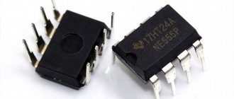
Every radio amateur has encountered the NE555 chip more than once. This little eight-legged timer has gained enormous popularity for its functionality, practicality and ease of use. On the 555 timer, you can assemble circuits of various levels of complexity: from a simple Schmitt trigger, with just a couple of elements, to a multi-stage combination lock using a large number of additional components.
In this article, we will take a closer look at the NE555 microcircuit, which, despite its advanced age, is still in demand. It is worth noting that this demand is primarily due to the use of ICs in circuitry using LEDs.
Description and scope
The NE555 wiring or terminal designation has not changed for 50 years. The classic circuits in the plastic DIP-8 housing are decorated with the installation of SOP-8 and SOIC-8. The low price and availability of the circuit, ease of implementation and functionality make it possible to create complex electronic circuits. Without in-depth knowledge, the NE555 becomes a toy or a pirate metal detector. It all depends on the desire of the radio amateur, what he wants to get from the product.
Structured integrated circuit inside a chip
So, the process of creating an integrated circuit begins with a single silicon crystal, shaped like a long solid pipe, “cut” into thin disks - plates. Such wafers are laid out into many identical square or rectangular areas, each of which represents one silicon chip (microchip). An example of the internal structure of an integrated circuit, demonstrating the capabilities of such a unique technology for integrating full-fledged electronic circuit solutions.
Thousands, millions, or even billions of components are then created on each chip by doping different areas of the surface into N-type or P-type silicon. Alloying is carried out in various ways. One option is sputtering, when a silicon wafer is “bombarded” with ions of the dopant material.
Another option is vapor deposition, which involves introducing an alloying material in the gas phase followed by condensation. As a result of this introduction, impurity atoms form a thin film on the surface of the silicon wafer. Molecular beam epitaxy is considered the most accurate deposition option.
Of course, the creation of integrated circuits, where hundreds, millions or billions of components are packed into a silicon chip the size of a fingernail, seems to be a very complex process. One can imagine what chaos even a small grain will bring when working on a microscopic (nanoscopic) scale. This is why semiconductors are manufactured in squeaky clean laboratory conditions. The air in laboratory rooms is carefully filtered, and workers must pass through protective airlocks and wear protective clothing.
Who created the integrated circuit?
The development of the integrated circuit is credited to two physicists, Jack Kilby and Robert Noyce, as a joint invention. However, in fact, Kilby and Noyce hatched the idea of an integrated circuit independently of each other. There was even a kind of competition between scientists for the rights to the invention.
Jack Kilby was working at Texas Instruments when the scientist managed to realize the idea of a monolithic principle of placing various parts of an electronic circuit on a silicon chip. The scientist manually created the world's first integrated circuit (1958), using a germanium-based chip. a year later she filed a patent application.
Meanwhile, a representative of the other, Robert Noyce, conducted experiments with miniature circuits of his device. Through a series of photographic and chemical techniques (the planar process), Kilby created a practical integrated circuit just a year later. The production method was also filed for a patent.
Microcircuits on the board
Main parameters of the 555 series IC
The product operates properly when the electrical specifications for the signal input and output are maintained. Examples of parameters are summarized in a standard series, where the extreme values show the range and tolerances:
- Voltage level at pin (V) THRES (VCC15) – 8.8–11.2.
- Also at VCC (5V) – 2.4–4.2.
- The current at the THRES pin (A) is 30 x 10-9 and 250 x 10-9.
- The potential at the TRIG pin (V) at VCC15V is 4.5-5.6; VCC 5V 1.1–2.2.
- The remaining operating parameters are in picture 2.
Let's move from theory to practice
Bipolar transistors: switching circuits. circuit diagram for connecting a bipolar transistor with a common emitter
I assembled a Tesla generator into an ATX housing. Power supply capacitor 1000 uF 400V. Diode bridge from the same ATX at 8A 600V. I placed a 10 W 4.7 Ohm resistor in front of the bridge. This ensures smooth charging of the capacitor. To power the driver, I installed a 220-12V transformer and a stabilizer with a 1800 uF capacitor.
I screwed the diode bridges onto the radiator for convenience and for heat removal, although they barely heat up.
The breaker was assembled almost like a canopy, took a piece of PCB and cut out the tracks with a utility knife.
The power unit was assembled on a small radiator with a fan; it later turned out that this radiator was quite sufficient for cooling. The driver was mounted above the power one through a thick piece of cardboard. Below is a photo of the almost assembled design of the Tesla generator, but it is being tested; I measured the power temperature in various modes (you can see an ordinary room thermometer attached to the power one on thermoplastic).
The coil toroid is assembled from a corrugated plastic pipe with a diameter of 50 mm and covered with aluminum tape. The secondary winding itself is wound on a 110 mm pipe 20 cm high with 0.22 mm wire about 1000 turns. The primary winding contains as many as 12 turns, made with a margin in order to reduce the current through the power section. I did it with 6 turns at the beginning, the result is almost the same, but I think it’s not worth risking transistors for the sake of a couple of extra centimeters of discharge. The frame of the primary is an ordinary flower pot. From the beginning I thought that it would not pierce if I wrapped the secondary with tape and the primary on top of the tape. But alas, it did. Of course, it also broke in the pot, but here the tape helped solve the problem. In general, the finished design looks like this:
Well, a few photos with the discharge
Now everything seems to be done.
Location and assignment of pins
The pin locations are indicated by terminals:
- GND – (ground, minus).
- Trigger – (opening).
- Output – (output signal).
- Reset – (reset parameters).
- Control Voltage – (control).
- Threshold – (stop).
- Dischage – (discharge).
- Vcc – (plus, power supply).
The first mark is marked with a circular indentation or bulge on the body.
Bipolar voltage switching power supply circuit
It is assembled on a single NE555 chip (Fig. 1), which serves as a master generator of rectangular pulses. The generator is assembled according to the classical scheme. The generator output pulse repetition rate is 6.474…6.37 kHz. It varies depending on the supply voltage, which can be 3.6 V (3 batteries in a power cassette) and 4.8 V (with 4 batteries in a power cassette). In the switching power supply circuit, ENERGIZER AA batteries with a capacity of 2500 mAh were used. Rectangular pulses from output 3 of MS 555 are fed through limiting resistor R5 to the base of transistor switch VT1, the load of which is inductor L1 with an inductance of 3 mH. When this transistor is abruptly closed, a large self-induction EMF is induced in inductor L1. The high-voltage pulses obtained in this way are supplied to two parallel rectifiers with voltage doubling, the outputs of which will have two opposite-polar voltages ±4.5...15 V.
These voltages can be adjusted by changing the duty cycle of the output pulses using potentiometer R1. The constant voltage from the R1 engine reaches pin 5 of the MC555 and changes the duty cycle, and therefore the output voltage of both rectifiers. The output voltages of this source will be ideally equal only if the duty cycle of the generator pulses is equal to 2 (the duration of the pulses is equal to the pause between them)
With a different duty cycle of the pulses, the output voltages of the source at points A and B will differ slightly (up to 1...2 V). Such a small difference is ensured by the use of doubling rectifiers in the switching power supply circuit, the capacitors of which are charged by both positive and negative pulses. This disadvantage is compensated by the simplicity and low cost of the scheme.
In this switching power supply circuit, you can use chokes from electronic ballasts of unusable energy-efficient fluorescent lamps. When disassembling these lamps, be careful not to damage the spiral or U-shaped glass tubes, as they contain mercury. It is better to do this outdoors. On some chokes, especially imported ones, the inductance value in mH is marked (2.8, 2.2, 3.0, 3.6, etc.). Input and output voltages, current consumption and pulse repetition rates for the circuit in Fig. 1 are given in Table 1.
Operating modes
Input (2) receives and processes single-cycle pulses. When the microcircuit is switched, a high signal level appears at the output (3). The duration of the pulses (seconds) reaches: t=1.1*R*C. As the time interval (t) passes, low-level signals are generated at the output. It is advisable to combine conclusions 4 and 8.
One-shot
The NE555 MK is shown in the picture; it produces a voltage at the OUT output equal to the IP potential minus 1.7 Volts. For example, 5-1.7 = 3.3V minimum. 15-1.7=13.3 maximum. This happens for a period of time until the IN input is closed to “0” (ground).
Important! Radio amateurs take into account that R1 is selected for 10 kOhm - 15 MOhm (less often 300 kOhm), the second aspect of C1 is 95 pF. In this case the delay circuit is 1.1 sec.
Multivibrator
In multivibrator mode, our microcircuit produces rectangular signals with a given frequency. The frequency of each pulse determines the value of the timing RC chain. With the addition of 1 resistance, pin 7 (discharge) connected between resistors Ra and Rb, logically turns off the universal timer inside.
Important! The frequency cannot be kept above 360 kHz; this will immediately lead to damage to the device.
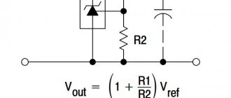
Precision Schmidt trigger with rs trigger
A high level of accuracy is achieved when a SCHMITT trigger is performed based on a COMPARATOR with an analog switch. The output voltage “Ue” is kept such that it does not exceed the lowest values:
\[Ue on = (R1/R2) * Ua min \]
The rule is mandatory for startup and allows the assembly to function efficiently and reliably according to the variant of the precision Schmitt trigger.
The trigger is a radio-electronic element; it is in 2 states. The transition from state 1 to state 2 occurs when the input signals change. Triggers are used for pulse counters, frequency dividers, and other assemblies. The initial position occurs through 3 terminals, control. Input E (timer pin 4) is important and of paramount importance. Used to pause operation and reset RS trigger values.
Truth table of RS flip-flop.
| R | S | Q(t) | Q(t+1) | Explanations |
| 0 | 0 | 0 | 0 | Information storage mode R=S=0 |
| 0 | 0 | 1 | 1 | |
| 0 | 1 | 0 | 1 | Unit setting mode S=1 |
| 0 | 1 | 1 | 1 | |
| 1 | 0 | 0 | 0 | Zero recording mode R=1 |
| 1 | 0 | 1 | 0 | |
| 1 | 1 | 0 | * | R=S=1 prohibited combination |
| 1 | 1 | 1 | * |
DIY time relay on a 555 timer
08/31/2012 Electronic equipment
In the video tutorial of the channel “homemade products and reviews of packages from jakson” we will assemble a time relay circuit based on a timer chip on NE555. Very simple - few details, it will be very easy to solder everything with your own hands. Along with this, many will need it.
Radio components for time relays
The microcircuit itself, two simple resistors (one variable, one polar), a 3 microfarad capacitor, a 0.01 µF non-polar capacitor, a KT315 transistor, almost any diode, one relay will be useful. The device supply voltage will be from 9 to 14 volts. You can purchase radio components or a ready-made time relay in this Chinese store.
A plugin for Google Chrome to save money: 7 percent of purchases are returned to you.
The scheme is very simple.
Time relay circuit on a 555 timer
Anyone can master it, given the necessary details. Assembly on a printed circuit board, which makes everything compact. As a result, part of the board will need to be broken off. A simple button without a lock will come in handy; it will activate the relay.
In addition, there are two variable resistors, instead of one, which is required in the circuit, because the master does not have the required value.
2 megaohms. Two 1 megaohm resistors in series. In addition to this relay, the supply voltage is 12 volts DC, and can pass through itself 250 volts, 10 amperes alternating current.
Upon completion of assembly, this is what a time relay based on a 555 timer looks like.
Everything turned out to be compact. The only thing that visually spoils the appearance is the diode, because it has such a shape that it is impossible to solder it otherwise, because its legs are much wider than the holes in the board. It still turned out to be good enough.
Checking the device on a 555 timer
Let's make sure the domestic relay is reliable. The operation indicator will be an LED strip. Let's also connect a multimeter. Let's make sure it's reliable - press the button, the LED strip lights up. The voltage supplied to the relay is 12.5 volts. The voltage is currently zero, but for some reason the LEDs are on - probably a relay malfunction.
It is old, soldered from an unnecessary board.
By transforming the position of the trimming resistors, we can adjust the operating time of the relay. Let's measure the large and minimal time. It turns off almost immediately. And big time.
About 2-3 minutes passed. - you can see for yourself.
But such indicators are only in the presented case. Yours may be different, because it depends on the variable resistor that you will use and on the capacitance of the electric capacitor. The larger the capacity, the longer your time relay will work.
Analogs
Since 1975, the KR1006VI1 series product has been created as an analogue. The production of the design continues in Riga (Republic of Latvia). Production by Belarus has also been preserved since the post-Soviet period (USSR). Their production “Integral” continues to produce products, only the marking makes it distinctive, the IN555 series.
Note! The product KR1006VI1 in Russian completely repeats the English versions (datasheet 555).
Manufacturers
The considered universal timer, created by the American company Signetics back in 1971, still continues to be produced by almost all well-known global brands in the semiconductor industry. At the same time, the labeling of its complete analogues from different companies may differ from the original, despite complete functional and physical identity. For example, judging by the datasheet NE555 P (aka LM555P) and NE555N are the same device from two competitors: Texas Instruments and STMicroelectronics, respectively. NE555L is a product of China's Unisonic Technologies Co (UTC). Japanese Motorola once made CMOS versions with the designation MC1455. Currently, the process of its improvement and modernization to meet modern requirements continues.
The most popular circuits based on ne555
Dimensions of different types of housing designs, and with the number of terminals 8, there are only 4 options (dimensions shown in mm):
- PDIP (9.81 – 6.35).
- SOP (6.20 – 5.30).
- TSSOP (3.00 – 4.40).
- SOIC (4.90 – 3.91).
An interesting design can be obtained by assembling a metal detector for 1 MK IN 555. A small number of radio components will be required. The diameter of the coil is no more than 70–90 mm with 250–290 turns of wire. They make varnish insulation of the winding (PEL, PEV), with a copper diameter of 0.4 mm. Instead of the speaker, headphones and a piezo emitter are suitable. The diagram is in the picture.
Flashing LED on the multivibrator
There are dozens of multivibrator circuits, so the screenshot shows one simple option. This one shows the assembly of an astable symmetrical multivibrator. This is usually how radio amateurs do it. FLASHER - it is soldered using the most readily available radio components. Whatever is found in stock is used in the assembly.
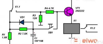
Time relay
The time relay circuit is simple. The classic version can be repeated by a home specialist.
The device is started with toggle switch SB1. Resistor R2 is responsible for the duration of the signal. The average response time reaches 6 seconds. To increase the time, the capacity on R2 is increased. This is done with capacitor C1 and by selecting a parameter. What do you need? A typical electrolytic capacitor is 1600 µF.
The calculation is as follows: T=C1*R2, where C1 capacity is 1600 and R2 is the average resistance megohm.
Musical keyboard
The simplest solution is to collect a child's organ. Children and adults will like the toy. Moreover, this requires simple assembly and soldering.
Timer
The diagram is simple, in the sketch. Proper assembly does not require any configuration.
Important! Connecting pin 2 with pin 4 does not turn on the device; according to the indicated diagram, replace terminal 2 with pin 6.
Car alarm simulator
The signaling device works like a decoy (the light simply blinks at a frequency similar to a real alarm). You will need 12 V for power. The diagram shows a mode switch, in the first the LED just lights up, in the other it blinks. A very simple circuit, ideal for beginner radio amateurs.
A simple police siren simulator
The tone of the siren is changed by a potentiometer on a 100 kOhm resistor between pins 6 and 7. The values of the remaining parts are shown in the sketch. The device control is changed by the voltage at pin 2 (from 2.5 to 5V). Check the functionality by connecting to a voltmeter or oscilloscope. The oscillograms move smoothly both up and down. An analogue of a buffer cascade between 2 timers is assembled on the KT361 transistor.
Liquid Level Sound Generator
It is more clear to see the invention of the liquid level on the roller. The weak point is the positive electrode, it begins to quickly dissolve (electrolysis effect). Graphite or stainless steel extends the life of the structure.
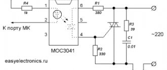
Dark alarm
The implementation of the assembly is shown in the screenshot. The darkness alarm circuit emits an audible signal when darkness falls. The beginning of the photoresistor is set by darkness. The photo relay is not illuminated when pin No. 4 is at a low voltage level. The timer is in reset mode. There is no lighting - the resistance on the photoresistor increases, a high level appears at pin No. 4, which starts the timer. When started, the timer emits a signal.
Friday, January 3, 2014
DIY time relay 2 (at 555).
To calculate the delay, you can use the program:
Advanced noise-resistant circuit without transistor:
You can read more about the improved scheme on the page https://electe.blogspot.ru/2016/03/555.html.”
Limits of permissible values
There are a number of typical maximum operating specifications for the NE555. They are found in the most common modifications of this microcircuit. Their differences depend only on the manufacturing company, but, as a rule, are the same in most technical descriptions:
The voltage of the energy source is from 4.5 to 18 Volts.
Power dissipation: 600 microwatts.
The output current is 200 milliamps.
Operating frequency - 500 kilohertz.
Temperature for operation - from 0 to 70 degrees, for storage - from -65 to 150 degrees.
If the specified parameters are exceeded, the device may fail.