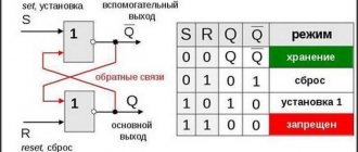
Triggers of various types are often included in various simple circuit designs that do not require the use of microcontrollers. They can save previously set values, change them, and record a logical zero or one. The D-trigger is one of the most common types of such devices. It allows you to delay signals, as well as store information for the required time.
What are the triggers?
The action of triggers is based on certain principles, depending on their type. These logic devices receive input signals that control them. The output information depends on the signal received at the input and on the one received at the previous stage. Consequently, the D-flip-flop reacts both to currently existing values and to previously received ones.
The graphical designation (UGO) of a D-flip-flop demonstrates that its input D is informational, and the second, designated by the letter C, is used to synchronize recording and allows you to save at the output the state that was at the input at the time it changed to 1 (which called "transparency" mode).
A trigger can be synchronous (clocked) or asynchronous (unclocked). In the first case, the device takes into account clock signals. In any computing system, all actions are performed in relation to signals of this type in order to ensure consistent operation.
The use of clock signals in synchronous flip-flops means that operation according to the underlying principle does not occur at any time, but only when a certain event is observed at the control input. For example, if a clock pulse transitions from the maximum value to zero or vice versa. Asynchronous devices do not have such a binding. In them, the transition from one mode to another is accomplished by a voltage drop.
Triggers are quite complex electronic circuits, but they provide a simple and understandable principle for converting input signals into output signals. D-flip-flops are also called “latches,” which clearly explains their operating principle.
The signal propagation delay time in a push-pull trigger is at least: 6*tз.
| S | & 1 | & 1 |
| & | & | |
| C | ||
| & 1 | & 1 | |
| R | & | & |
| Decrease | time | |||
| delays | distribution | |||
| Q | signal | at | two-stroke | |
| trigger | Can | due to | ||
| applications | two | fast- | ||
| existing | single-cycle | |||
| RS triggers. Availability | ||||
| second | inverse trigger | |||
Qsync input “C” allows
implement the minimum delay time: 4*tз.
T-trigger
Based on the RS flip-flop, you can implement a T-trigger (counting trigger), i.e. a trigger that changes its output state at the edge of a pulse at input C. To do this, it is necessary to combine the output of the flip-flop Q with the input R, and the output ~Q with the input S.
| D1 | D3 | D5 |
| & | & | & |
| WITH | ||
| D2 | D6 | |
| & | & | & |
| D4 |
| D7 | Q | WITH | Q | ~Q |
| ~ — | — | |||
| & | ↓ | Q | Q |
To build a T-trigger, a push-pull trigger is fundamentally required. The first flip-flop stores the inverse state of the second flip-flop for one logical level at input C. After changing the logical level at input C (i.e., along the edge of the signal), the state of the first trigger is rewritten - into the second (the state is inverted
| output trigger). | ||
| The maximum input frequency of the T flip-flop is determined by | ||
| signal propagation delay time at the source | ||
| push-pull RS trigger: | ||
| • | , | Fmax 1 / (6 tЗ) |
where tз is the average propagation delay time of the signal of one logical element.
The great similarity between the state tables of the RS flip-flop and the J-K flip-flop is reflected in the great similarity of their circuit diagrams
In accordance with the state table, when logical units are applied to inputs J and K (last row of the table), this flip-flop operates as a T-flip-flop, i.e. inverts its state on each edge (in this case, the falling edge) of the signal at input C.
JK trigger is fundamentally push-pull
trigger, since to invert the output state it is necessary to remember the previous state of the trigger.
Questions for express control
•1. Name the main states of the trigger.
•2. What are the disadvantages of an asynchronous trigger?
•3. What are the advantages of a synchronous trigger over an asynchronous one?
•4. What is the difference between potential triggers and potential triggers?
front?
•5. How can you change the direction of the front?
trigger synchronization?
•6. What is the definition of propagation delay?
signals in triggers?
Questions for express control
• 7. What is the difference between R-S and J-K flip-flops?
•8. What is a counting trigger? How can you implement a counting flip-flop based on R-S-, D-,
•JK flip-flops?
•9. Is it possible to implement a counting trigger based on
single-ended trigger?
•10. What determines the maximum frequency
counting trigger?
LECTURE IS OVER
THANK YOU FOR YOUR ATTENTION
studfiles.net
How does a D-trigger work?
The D-trigger inputs are divided into information (control) and auxiliary. The latter are designed to synchronize the operation of the device. The first set a certain combination of binary numbers at the input, which will be taken into account when generating the output signal. The clock signal controls the operating logic. It is he who determines the moment the trigger is triggered, and the state of the output signal depends on its characteristics.
A D flip-flop is also called a delay flip-flop because it is capable of delaying the input information signal by one clock cycle. The delay time is determined by the frequency of the synchronization pulses. If the information signal changes, the output will repeat its change, but only after the clock signal takes a value equal to one. As long as its value remains zero, the output signal will not change.
The operation of any D flip-flop is reflected in the truth table. As you can see, the truth table of a static D flip-flop is quite simple. It shows that a zero value of the control signal ensures that the previous value of the output signal is stored for any desired period of time. In practice, we are talking about the time when power is connected to the device.
The presented truth table provides information about the operation of a D-flip-flop at a value of C = 1. In practice, another option is used when operation occurs on the leading edge of the pulse. That is, the output value becomes equal to the input value at the moment when the value of the control pulse changes from zero to 1. A logic element that uses control by voltage level is called a static D-trigger, and by the edge - dynamic.
When edge control is used, triggering occurs when the control value changes. Two options can be used: leading edge or trailing edge. When using the first option, the value changes from 0 to 1, the second - from 1 to 0.
In addition to the table, timing diagrams are also used to describe the operation of logical elements.
• Single-ended and push-pull triggers
Rice. Single-ended JK trigger and its symbolic designation
•Triggered at the moment the strobe signal C transitions from 0 to 1 (along its leading edge).
State table of single-ended jk flip-flop
•If you connect inputs j,c and k, you get a T-flip-flop.
•If c = 0, then storage for any J and K.
•There are no forbidden states in the jk trigger
| state | |||||
| Jn | Kn C | Qn+1 | Qn 1 | ||
| 0 | 0 | Qn | Qn | storage | |
| 0 | 1 | 0 | 1 | entry 0 | |
| 1 | 0 | 1 | 0 | entry 1 | |
| 1 | 1 | Qn | Qn | T-trigger | |
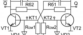
Push-pull (2-stage) triggers
1) Push-pull RS trigger(MS trigger)
When C = 1, information is received in the M flip-flop, but does not pass into the S flip-flop.
When C = 0, information from the M-trigger is rewritten into the S-trigger.
| M – master – | S – slave – |
| leading | slave |
| For any C one step | trigger “transparent”, other |
“opaque”, so the trigger as a whole is opaque.
•Pull-pull JK trigger
This is a push-pull RS flip-flop, the Q outputs of which are connected crosswise to the input connectors, then the R and S inputs are called J and K inputs.
If j = k = 0 then the C signal cannot open the flip-flop - storage.
If j = 1;k = 0, then the C signal will open the connector &1, but only if before the C signal arrived there was: Q = 0;
•Unlike a regular RS trigger, the option j = k = 1 is not prohibited.
TOPIC 2. Registers.
Classification of registers.
Parallel and serial registers.
Paraphase and single-phase registers. Shift registers.
A register is a functional unit that unites several
triggers of the same type
•Register types:
•Latch registers – are built on latched triggers (K155TM5; K155TM7), which are written to by the level of the strobe signal.
•In the K155TM8 trigger – recording is carried out by the positive edge of the strobe signal.
•Shift registers – perform the function of sequential code reception only.
•Universal registers – can receive information in parallel and serial code.
•Special registers – K589IR12 have additional
•use options.
•Shift register
•This is a register, the contents of which, when a control signal is applied, can be shifted towards the higher or lower digits. For example, a left shift is shown in Table 9.
Table 9 Code shift left
•Register with single-phase synchronization.
In a register with single-phase synchronization, at the moment the strobe pulse arrives, the input bit DS is written to the trigger TT0. The information available in TT0 is copied into the trigger TT1, into TT2 from TT1, etc.
• The DS input receives a serial code.
•When the next DS bit and signal C are applied, the same process occurs, as a result, all the bits present at the outputs Q0-Q3 are moved 1 bit to the left. The symbol for such a register is shown in the figure.
Symbol
Shift register (symbol)
•Two-phase shift register
In a two-phase register, signal C1 is used to write to single-ended flip-flops T00 and T01, and signal C2 sends information to flip-flops T10 and T11 and appears at outputs Q0 and Q1. Shift registers are used to convert serial code into parallel.
Topic 3. Counters
Classification of meters. Synthesis of counters. Binary counters.
Counters with variable counting module.
Adding, subtracting and reversing counters
•Classification of meters
•Counter is a functional unit intended for counting
signals. As input signals arrive, the counter sequentially cycles through its states in an order specific to a given circuit. For example:
•The length of the list of used states K is called the conversion module or the counter capacity.
•The most commonly used binary counters have a rotation order
trigger states corresponds to a sequence of binary codes.
•Other types of coding are also used, for example single, when the state of the counter is determined by the location of the moving unit.
•Unitary encoding – state
determined by the number of units
studfiles.net
A more complicated version of the trigger
Sometimes a more complicated version is used when another input is added. It is usually designated by the letter R. If a signal with a zero value is applied to it, it has no effect on the operation of the element. In the case when a signal with a single value is received at input R, Q is reset to 0. The same can be achieved on a classic D flip-flop if you use C = 0 and D = 0.
D-flip-flop implementation schemes
There are different options for constructing this logical element. Below is a diagram of a single-stage D flip-flop using NAND elements. Its inputs are direct static. The elements designated DD1.1 and DD1.2 are involved in the control circuit, and the rest are used as an asynchronous RS trigger.
The role of each element will be easier to understand by studying the principle of operation of the D-trigger. From the diagram it can be seen that if C = 0, then the logical AND operation will create a zero value regardless of the second input values on DD1.1 and DD1.2. The negation operation will produce a one at the output of both of these elements.
At the input of the third element there will be two values: one and the negation of Q. The AND operation at the output will form the negation of Q. The negation will lead to the fact that the output will have a Q value that coincides with the one that was here before.
The fourth element will receive one and Q. The result of applying AND will be Q. After applying negation, the output of this element will be the negation of Q. Therefore, in this case the value will not change.
Now we need to consider the situation when the control input has a single value. If D = 0, then after applying AND a zero will be obtained, and as a result of negation, the output value of DD.1 will become one, which will be transmitted to the input of DD1.2.
In DD1.2 there are two ones at the input, which means the AND operation will generate 1, and negation will give 0. Therefore, at DD1.4 the output will be one, which corresponds to a zero value of Q. The remaining options are calculated using the same principle.
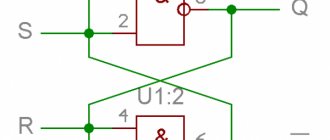
The D-trigger circuit can be obtained from a synchronous RS-trigger by introducing an additional AND-NOT element, connecting both inverse inputs into one information input. This eliminates the state of uncertainty for S and R.
There are also combined D-triggers. They have inputs S and R, intended for asynchronous setting of logical 0 and 1. Using these inputs, the device can be given an initial specific state.
The diagram shows that a D-flip-flop is built from 6 AND-NOT elements; its operating principle is as follows: if there is a 1 at the input R and a zero at C, D, S, elements from the first to the fifth will remain closed. The sixth element will be open, that is, Q = 1, and /Q = 0. The first element will open if the zero signal is removed from the S input. The state of the remaining elements will not change.
When a single signal arrives at input C, the same signal will appear at all inputs of the third element, causing it to open. The sixth element will close and /Q = 1. Then single signals will also arrive at the inputs of the fifth element, and it will assume an open state, and Q = 0. As a result, after switching the trigger, a signal identical to the signal that was at the input will appear at the output Q D before switching, that is, Qn+1 = Dn = 0. If a single signal is removed from input C, the state of the trigger does not change.
The D-trigger circuit is quite simply implemented on CMOS chips. In such devices, the functions of logical elements AND are performed by ordinary transistor switches.
After a high-level clock signal arrives at input C, transistor No. 1 opens, providing a signal from D to Q. This activates the first inverter. In this situation, the second transistor remains closed. It turns off the inverter, built on transistors VT1 and VT3. This inverter turns on after a low potential arrives at input C.
D-flip-flops are included in many microcircuits. For example, the TM2 chip contains two such elements, TM5, TM7, TM8 - four, TM9 - six.
• Single-ended and push-pull triggers
Rice. Single-ended JK trigger and its symbolic designation
It is triggered at the moment the strobe signal C transitions from 0 to 1 (along its leading edge).
State table of single-ended jk flip-flop
•If you connect inputs j,c and k, you get a T-flip-flop.
•If c = 0, then storage for any J and K.
•There are no forbidden states in the jk trigger
| state | |||||
| Jn | Kn C | Qn+1 | Qn 1 | ||
| 0 | 0 | Qn | Qn | storage | |
| 0 | 1 | 0 | 1 | entry 0 | |
| 1 | 0 | 1 | 0 | entry 1 | |
| 1 | 1 | Qn | Qn | T-trigger | |
Push-pull (2-stage) triggers
1) Push-pull RS trigger(MS trigger)
When C = 1, information is received in the M flip-flop, but does not pass into the S flip-flop.
When C = 0, information from the M-trigger is rewritten into the S-trigger.
| M – master – | S – slave – |
| leading | slave |
| For any C | one trigger stage is “transparent”, the other |
“opaque”, so the trigger as a whole is opaque.
•Pull-pull JK trigger
This is a push-pull RS flip-flop, the Q outputs of which are connected crosswise to the input connectors, then the R and S inputs are called J and K inputs.
If j = k = 0, then the C signal cannot open the storage flip-flop.
If j = 1; k = 0, then the C signal will open the connector &1, but only if before the C signal arrived there was: Q = 0;
•Unlike a regular RS trigger, the option j = k = 1 is not prohibited.
TOPIC 12. Registers.
Classification of registers.
Parallel and serial registers.
Paraphase and single-phase registers.
Shift registers.
A register is a functional unit that unites several
triggers of the same type
Register types:
Latch registers are built on latched triggers (K155TM5; K155TM7), which are written to by the level of the strobe signal.
In the K155TM8 trigger, recording is carried out by the positive edge of the strobe signal.
Shift registers - perform the function of only sequentially receiving code.
Universal registers - can accept information in parallel and serial code.
Special registers - K589IR12 have additional
use cases.
•Shift register
This is a register, the contents of which, when a control signal is applied, can be shifted towards the higher or lower digits. For example, the left shift is shown in Table 9.
Table 9 Code shift left
•Register with single-phase synchronization.
In a register with single-phase synchronization, at the moment the strobe pulse arrives, the input bit DS is written to the trigger TT0. The information available in TT0 is copied into the trigger TT1, into TT2 from TT1, etc.
The DS input receives a serial code.
•When the next DS bit and signal C are applied, the same process occurs, as a result, all the bits present at the outputs Q0-Q3 are moved 1 bit to the left. The symbol for such a register is shown in the figure.
Symbol
•Shift register (symbol)
Two-phase shift register
In a two-phase register, signal C1 is used to write to single-ended flip-flops T00 and T01, and signal C2 sends information to flip-flops T10 and T11 and appears at outputs Q0 and Q1. Shift registers are used to convert serial code into parallel.
Topic 13. Counters
Classification of meters.
Synthesis of counters.
Binary counters.
Counters with variable counting module.
Adding, subtracting and
reversible counters
•Classification of meters
Counter - a functional unit intended for counting
signals. As input signals arrive, the counter sequentially cycles through its states in an order specific to a given circuit. For example:
•The length of the list of used states K is called the conversion module or the counter capacity.
•The most commonly used binary counters have a rotation order
trigger states corresponds to a sequence of binary codes.
•Other types of coding are also used, for example single, when the state of the counter is determined by the location of the moving unit.
•Unitary encoding – state
determined by the number of units
studfiles.net
Application of D-flip-flops
The ability to store information allows the use of D-flip-flops to implement memory devices. These operating elements are capable of maintaining the desired output mode until a control signal is applied to change it. A trigger makes it possible to both enter binary information and store and read it.
Understanding what a D flip-flop is, it can be used to create a latch register. These devices are important in certain situations. Sometimes the signal lasts for a very short period of time and the microcircuit may not have time to react to it. In such cases, it is advantageous to use another chip, which will store the necessary values for a time sufficient to perform the necessary actions.
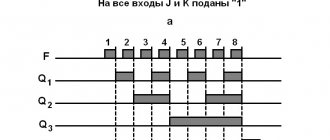
One of the main purposes of a D-flip-flop is to be used in counting mode. To make it work as a pulse counter, it is enough to apply a signal to input D from its own inverter output. In this mode, upon arrival of each pulse at input C, the trigger will change its state to the opposite, as shown in the timing diagram.
A frequency divider is a device that can change the frequency of the output signal relative to the input value. Using a cascade connection of several elements, it is possible to build frequency dividers with different division ratios. Two D flip-flops connected in series produce an output signal that is one-fourth the frequency of the input. Three elements connected in series will divide it by eight, and four elements will divide it by sixteen.
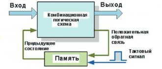
When creating digital circuits, the operation of which is synchronized by a single clock generator, it is often necessary to achieve synchronization of the operating circuit and the external input signal. That is, an asynchronous signal must be converted into a synchronous one for the entire system into which it enters. This problem can be solved by installing a D-trigger.
A trigger is capable of performing a logical function and at the same time maintaining feedback. That is why it is used to create many devices designed to remember, store, transmit and convert information. These elements can be found in a wide variety of devices, including digital microelectronics devices.