Many electronic components are sensitive to static electricity, moisture and mechanical damage. This is especially true for microcircuits, because their logic is located on a fragile semiconductor crystal or film. The case in this case is an integral part of the microcircuit design, protecting it from external influences. In addition, it also has a connecting function, connecting the microcircuit with other components of the electronic device into which it is integrated.
In order to simplify the process of assembling products, microcircuit packages are standardized according to a number of characteristics. Today you can buy microcircuits in hundreds of different cases, so to simplify the selection, they are all divided into series and labeled. Below are a series of foreign-made microcircuits that are most widespread in our latitudes.
DIP
One of the most common cases today. Used to protect multi-pin microcircuits and some other electronic components (LEDs, switches, all kinds of sensors). It can have from 4 to 48 pins placed in parallel along the edges of the case. The case itself is made in the shape of a rectangle and is mounted by soldering the pins into the board or by installing it into the receiving connector. In addition to standard plastic (PDIP), there are also more reliable ceramic housings (CDIP).
DIP chip package drawings
Chip types
Currently, a huge number of types of microcircuits are produced. Almost any complete electronic component, standard or specialized, is available in a micro version. It is not possible to list and analyze all types within one review. But in general, based on their functional purpose, microcircuits can be divided into three global categories.
- Digital. Work with discrete signals. Digital levels are supplied to the input, and signals in digital form are also taken from the output. This class of devices covers the area from simple logic elements to the most modern microprocessors. This also includes programmable logic matrices, memory devices, etc.
- Analog. They work with signals that change according to a continuous law. A typical example of such a microcircuit is an audio amplifier. This class also includes integrated linear stabilizers, signal generators, measuring sensors and much more. The analog category also includes sets of passive elements (resistors, RC circuits, etc.).
- Analog-to-digital (digital-to-analog). These chips not only convert discrete data into continuous data or vice versa. Source or received signals in the same package can be amplified, converted, modulated, decoded, etc. Analog-to-digital sensors are widely used for connecting the measuring circuits of various technological processes with computing devices.
SOIC
Compact rectangular housing with terminals on the edges. Often labeled by manufacturers with the abbreviation SO or SOP. A microcircuit hidden in such a case can be twice as compact and take up half as much space on the board as if it were installed in a DIP. Another difference concerns the conclusions. As with DIP packages, they are located along the edges. But the petals soldered on the board are located in this case not perpendicular to the plane of the body, but parallel to it.
SOIC package drawings
Multi-chip modules (MCM)
Multi-chip modules belonged, until the early 1990s, to the areas of space and military technology and the high-end computer industry. IBM was the first to succeed in the practical use of MSM when organizing the production of a series of fourth-generation computers. Multilayer ceramic boards were used as a mounting and heat-dissipating base. A plant for their production was built especially for this purpose. A large amount of work is currently being carried out in Germany, in particular, at the University of Rostock and the Technical University in Berlin, where, through the use of MSM technologies, the layout is increased not only in the plane of the module, but also along its vertical (Fig. 9).
Rice. 9. Experimental samples of MSM elements at the Technical University of Berlin
In the 1990s, the use of MSM was the only solution to increase integration and correspondingly increase the functionality of the equipment. At that time, investments in the creation of multi-chip modules were less than investments in microelectronics.
But later, the development of electronics followed the now traditional path - along the path of increasing the integration of microcircuits, which entailed huge investments in their production. These trends can still be seen today. Chip factories built in Southeast Asia with topological resolutions of 0.065 microns and 0.093 microns are not yet fully loaded. Therefore, today efforts are focused on projects that would take advantage of the capabilities of developing microelectronic production.
However, MSM projects are being seriously developed where other ways of integration are not available for one reason or another.
The main difficulty in creating MSM is the difficulty in testing microcircuit crystals. If the probability of getting into the three-chip module is 95% of suitable microcircuits, the yield of suitable MSM is 85.7%. Next comes the question of identifying good and bad module components. The profitability of MSM production is directly related to the probability of suitable microcircuits.
Rice. 10
Rice. eleven
Rice. 12
Anyway, the most expensive part of MCM is the base (substrate). Table 1 shows the design options for MSM mounting bases. The MCM-L option is preferable from a cost-effective perspective.
Table 1. Modern ideas about multi-chip modules
QFP
Flat quadrangular surface mount housing. The conclusions are located at the edges. In many ways, a QFP package is similar to a SOIC, with the only difference being that the pins are located along all four sides, and not just along two.
Drawings of QFP, TQFP, LQFP chip packages
SIP
Convenient type of housing for vertical mounting on a board. The pins are located on one side, and the number after the abbreviation SIP indicates their number. Xilinx and other large manufacturers have HSIP modifications - this is a case of the same format, but equipped with a heat dissipator.
SIP chip package drawings
BGA components
BGA technology originated approximately 20 years ago at IBM for internal consumption. The first company to learn from IBM was Motorola, which bought a license from IBM and developed its technology into a package called OMPAC (Overmoulded Plastic Array Carrier). The structure of the BGA component is shown in Fig. 2.
Rice. 2. BGA component in a plastic case
According to this scheme, the crystal is mounted on a mounting substrate made of a composite material with an organic binder (FR-4, FR-5, BT) having a high glass transition temperature. For these purposes, it is preferable to use a material based on BT (Bismaleimid Triasine) with a particularly high glass transition temperature and excellent electrical properties. A NiAu finishing coating is applied to both sides of the substrate, which is universal for microwelding (welding wires from the microcircuit to the substrate) and soldering ball leads.
The crystal is glued to the substrate with a thermally conductive epoxy resin adhesive. In turn, the substrate has elements of conductive heat removal from one side to the other. Some of the ball leads are intended for thermal connections.
Modern standards set the pitch of the grid of matrix leads: 1.5 mm, 1.27 mm and 1.0 mm and the diameter of the ball leads is 0.6 mm. The designs of 50x50 mm substrates allow 2401 pins to be placed on them with a pitch of 1.0 mm.
Chip chips are mounted on a substrate using one of four methods:
- Thermocompression microwelding (wirebonding) is the oldest, most flexible and widely used method (Fig. 2). More than 96% of all microcircuits are still manufactured with its help.
- Attaching crystals to tape media terminals (Fig. 3), or TAB (Tape-automated Bonding). This method is used for automatic mounting of crystals with a small lead pitch onto an intermediate carrier. In addition to the possibility of automating installation, it provides the possibility of preliminary testing of crystals before final installation on the mounting substrate.
- Attaching an inverted crystal (Flip Chip) through ball terminals (Fig. 4). The compactness and improved electrical performance of this interconnection method are helping to expand its application.
Rice. 4. Installation of the microcircuit on the substrate using the inverted crystal method (Flip Chip)
- Connecting the crystal with beam leads (Fig. 5). This method uses technologies for thermocompression and ultrasonic microwelding of beam leads to peripheral contact pads on the chip and then beam leads to the substrate.
LCC
A compact low-profile case mounted in a specially equipped socket with contact petals on the sides (in common parlance - a “crib”). It is made of plastic (in this case marked with the abbreviation PLCC) or ceramics (CLCC). You can buy both types of microcircuits at all major electronic components stores, including ours.
Drawings of LCC, PLCC microcircuit packages
TSOP
One of the varieties of SOP enclosures, the distinctive feature of which is its small thickness. These packages often house low-voltage electronic components that are small in size and have a large number of pins (such as DRAM).
Drawings of TSOP chip packages
Structured integrated circuit inside a chip
So, the process of creating an integrated circuit begins with a single silicon crystal, shaped like a long solid pipe, “cut” into thin disks - plates. Such wafers are laid out into many identical square or rectangular areas, each of which represents one silicon chip (microchip). An example of the internal structure of an integrated circuit, demonstrating the capabilities of such a unique technology for integrating full-fledged electronic circuit solutions.
It will be interesting➡ What is the element base and where is it used
Thousands, millions, or even billions of components are then created on each chip by doping different areas of the surface into N-type or P-type silicon. Alloying is carried out in various ways. One option is sputtering, when a silicon wafer is “bombarded” with ions of the dopant material.
Another option is vapor deposition, which involves introducing an alloying material in the gas phase followed by condensation. As a result of this introduction, impurity atoms form a thin film on the surface of the silicon wafer. Molecular beam epitaxy is considered the most accurate deposition option.
Of course, the creation of integrated circuits, where hundreds, millions or billions of components are packed into a silicon chip the size of a fingernail, seems to be a very complex process. One can imagine what chaos even a small grain will bring when working on a microscopic (nanoscopic) scale. This is why semiconductors are manufactured in squeaky clean laboratory conditions. The air in laboratory rooms is carefully filtered, and workers must pass through protective airlocks and wear protective clothing.
Interesting read: what are klystrons.
Who created the integrated circuit?
The development of the integrated circuit is credited to two physicists, Jack Kilby and Robert Noyce, as a joint invention. However, in fact, Kilby and Noyce hatched the idea of an integrated circuit independently of each other. There was even a kind of competition between scientists for the rights to the invention.
Jack Kilby was working at Texas Instruments when the scientist managed to realize the idea of a monolithic principle of placing various parts of an electronic circuit on a silicon chip. The scientist manually created the world's first integrated circuit (1958), using a germanium-based chip. a year later she filed a patent application.
Meanwhile, a representative of the other, Robert Noyce, conducted experiments with miniature circuits of his device. Through a series of photographic and chemical techniques (the planar process), Kilby created a practical integrated circuit just a year later. The production method was also filed for a patent.
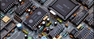
Microcircuits on the board
SSOP
Another type of SOP enclosure, characterized by even smaller dimensions. Designed for surface mounting. Well suited for compact chips with moderate heat dissipation. For hotter units, it is better to use TSSOP, since these cases have a larger area that can dissipate heat more efficiently.
Drawings of SSOP chip packages
ZIP
Very compact flat housing with zigzag contacts located at the bottom. You can buy microcircuits of this type in both standard and HZIP modifications (equipped with a heat dissipator).