Good afternoon friends!
Recently, you and I began to become more closely acquainted with how computer hardware works. And we met with one of his “building blocks” - a semiconductor diode. A computer is a complex system consisting of individual parts. By understanding how these individual parts (big and small) work, we gain knowledge.
By acquiring knowledge, we get a chance to help our iron computer friend if he suddenly goes haywire. We are responsible for those we have tamed, aren’t we?
Today we will continue this interesting business and try to figure out how perhaps the most important “building block” of electronics works - the transistor. Of all the types of transistors (there are many of them), we will now limit ourselves to considering the operation of field-effect transistors.
Principles of operation of field-effect transistors in electronic circuits: simplified information
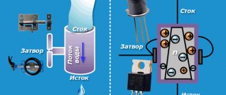
It is convenient to imagine all complex electronic processes using the example of an ordinary water tap with a handle that allows you to turn off the water or regulate its pressure from a very thin trickle (flow) to the strongest possible flow.
I showed this with a primitive picture in which:
- the inlet pipe with pressure is called drain;
- the place of water outlet (outflow) is indicated by the source;
- control handle or valve with a rod - shutter.
The electrical circuit of the field-effect transistor we are considering works in a similar way. Only it has the main constant voltage applied between the drain and source. This area is called a channel. It is made of a semiconductor of a certain structure:
- n-type (electrons predominate - carriers of negative charges);
- p-type - with an excess of positive holes.
In the drawings, these conclusions are shown in one of the following images.
On the shutter designation, we need to pay attention to the direction of the arrow. For n-channel semiconductors it is directed towards the gate, and with p-conductivity it is directed in the opposite direction.
Any field-effect transistors are semiconductors, and controllable ones at that. This means that it passes a load through itself exclusively in one direction, and the opposite movement of electrical charges is always blocked.
The movement of current through semiconductor junctions is always directed from drain to source, just like water in a tap. This is important to remember.
The functions of closing or opening this tap (gate), as well as the role of regulating the force of the flow of electrical charges, are assigned to the gate. Ohm’s well-known law applies here:
I=U/R
The resistance of the channel medium controls the load, and it is acted upon by an externally applied potential.
In other words: the electric field energy applied to the gate changes the resistance of the internal semiconductor junctions and affects the amount of current in the output power circuit.
The word “field” is significant here. It has defined a number of transistor products operating according to this control principle.
The electric field potential controls the amount of resistance across the power semiconductor layer (channel), turning the transistor off/on or changing the current through it.
Bipolar transistors (BTs), about which a previous article was published on my blog, are controlled in a similar way.
Only in them the power circuit is formed between the collector and the emitter, and the control circuit operates from the current generated by the application of voltage between the base and emitter. BT has its own pin designation system, but the same two internal circuits (power circuit and its regulation circuit).
I would like to draw your attention: at the same voltage between the input and output of the field-effect transistor (drain-source), the potential at the gate changes the electrical resistance of the built-in semiconductor junctions.
Moreover, this happens according to one of the scenarios provided in advance. I talk about them successively further.
Direct control from PWM controller
Most modern controller chips have a built-in output control stage. It usually contains a push-pull circuit with two transistors. This output can be used to directly drive the gate of a power field effect transistor, as shown in Fig. 1.
Rice. 1. Powerful DC is controlled directly from the output of the PWM controller
Direct connection can be used in cases where the control circuit is connected to the same ground as the power section and the power level is relatively small.
Judging by the reference data, a current of several amperes can be obtained directly from the output of the PWM controller. This is quite enough to control low-power devices. However, the FET input has a large capacitance. Also, trying to fully utilize all of the controller's output current is generally a bad idea. This can lead to increased EMI due to rapid turn-on and turn-off, excessive reverse recovery losses in the rectifier, and noise in the PWM controller itself. As a result, random glitches and clock jitter may occur.
The best solution is to limit the output current of the PWM controller using the circuit shown in Fig. 2. It uses two resistors, one to control the on time and the other to control the off time. (We usually turn the device off faster than we turn it on to protect against short current pulses.) The diode serves to separate these two functions, but in some cases where circuit performance is critical, you can do without it.
Rice. 2. Circuit with which you can limit the output current of the PWM controller
In low power converters, we usually turn on the DC voltage slowly. Don't be afraid to experiment with the resistance value of the Ron resistor. The author uses values from 1 Ohm to 1 kOhm in his projects. His design rule is to increase the resistance while monitoring the switching waveforms and power dissipation of the FET. If the temperature begins to increase noticeably, you need to reduce the resistance value by half. You will be surprised to see how slowly the DC can be turned on in a flyback converter operating in intermittent current mode without significant switching losses.
The switch-off must be fast to ensure a rapid decay of the current pulse. Experiment with different resistance values instead of just using the values given in the instruction manuals. More detailed information on how quickly the PT can be controlled can be found in [3].
How a field-effect transistor works: 6 types - brief information
The classification shown in the picture below, where their types are structured, will help us deal with a specific field grass and understand its structure.
JFET and MOSFET have different structure. In JFET, the gate (Gate) is directly built into the cross section of the channel and works as a control pn junction.
For mosfet:
- there is an additional fourth pin connected internally to the housing. It is not used when connecting to external circuits;
- The gate output region is separated by a layer of silicon dioxide (dielectric) from the channel semiconductor. It works as a plate capacitively coupled capacitor. Due to this modification, it is called an “insulated gate” or MOS transistor.
MIS stands for metal-dielectric-semiconductor and MOS stands for metal-oxide-semiconductor. The difference between them for a novice electrician is not significant, practically absent.
In the diagrams, mosfet and jifet are designated in different ways. MOSFET is drawn with:
- the fourth pin, which is not connected anywhere;
- a shutter separated from the main channel.
Mosfets are manufactured with different substrates (channels), which can be depleted or enriched in major charge carriers.
I will not describe and describe in more detail the differences between each type of these semiconductors for a novice electrician: there is not much point.
Below are just typical schedules of their work. They will give a general idea of behavior, and you will need to take specific data from the datasheet - technical documentation.
The amount of current flowing through the drain depends on the applied voltage between gate and source, as well as the ambient temperature.
The output drain current characteristics depend on the magnitude of the applied voltage between drain-source and gate-source.
This is how a MOS transistor with a built-in channel works. The current slope increases with increasing voltage Usi, Uzi.
And here are the characteristics of transistors with an induced channel.
Before any check of each transistor, it is necessary to clarify its technical capabilities according to the factory documentation.
Such graphical images and dependencies of electrical engineering processes, due to their clarity, have better information content.
6 features of electronic devices using MOSFETs
Recently, we are increasingly working with mosfet-type field devices with a channel of any conductivity.
Let us briefly analyze such a scheme and its properties.
Point No. 1: which shoulder to place the load on?
When the semiconductor junction is completely open, a very small resistance of tens or hundreds of milliOhms (Ropen) is created between the drain and the source, which forms a low voltage drop in this section (In · Roopen), where In is the value of the load current.
The voltage potential applied to the gate may not be sufficient to fully open the semiconductor. Therefore, the load is turned on higher on the drain side in an n-type field switch, and on the source side in a p-type field switch when the circuit is powered from a single source.
If the device uses additional voltage sources, then this requirement is not necessary.
Point No. 2: tricks for connecting a field worker to microcontrollers
For reliable operation of the MOSFET, it is necessary to apply a threshold voltage value between its gate and source (gate-source), which is indicated in the datasheet. It is usually around 10 volts. Still, digital devices work up to five: their power supply is not enough, you will need to add a level.
You can solve the problem in one of three ways:
- a key with bipolar transistors supplies the necessary power to the gate;
- connect a special driver (chip) to generate a control signal. They are designed for both the upper and lower shoulder to accommodate the load. Moreover, the high-side driver often uses a circuit to increase the output voltage;
- use a specialized low-level field operator (logic level). However, acquiring it can be problematic.
Point No. 3: how to avoid the influence of electrical interference
The appearance of any interference potential at the output of a transistor often leads to its unauthorized switching and disruption of electronic operating algorithms.
Therefore, the gate is always “pulled” to power or ground through a certain resistance, even when connected through a microcontroller. It should not be left in a free state, accessible to the penetration of extraneous interference.
Point No. 4: combating surge current when turned on
The natural presence of capacitance at the gate pin leads to a “current surge” each time the transistor is turned on. This can lead to damage to the semiconductor junction.
The problem is solved by introducing a resistor of sufficient value into the gate circuit. However, its value must be selected taking into account the increase in the key opening time.
Feature No. 5: inrush current protection when disconnecting inductive loads
A protective high-speed TVS diode, connected in parallel between the source and drain, reliably shunts the pulses created by disconnecting inductive loads.
When operating at high frequencies in bridge or half-bridge circuits of switching power supplies or induction heaters of hobs, a Schottky diode is connected counter-currently to the drain output, blocking the parasitic diode, because it increases the closing time, which can damage the semiconductor.
Point No. 6: additional MOSFET
Safe operation of a high-speed high-frequency switch in the switching mode of powerful inductive loads is ensured by its connection to snubber circuits. They:
- aperiodic currents created by transient processes close on themselves;
- reduce heating of semiconductors;
- protect the field switch from unauthorized opening during a rapid increase in voltage between drain and source.
Custom Gate Drivers
As the converter power increases, it becomes clear that the FET gate resistors must be reduced in order to minimize switching losses. For high power circuits in industry, as a rule, driver chips with high output currents are used. This reduces the influence of interference on the PWM controller, and, in addition, results in a more successful layout of the printed circuit board. There are many good drivers available for sale. You can even create your own powerful push-pull driver if you need to increase performance while lowering the price. For high power devices, a separate gate driver circuit is used to achieve fast switching (Figure 3). There are also resistors in the gate.
Rice. 3. Separate gate driver circuit for fast switching
How to solder field-effect transistors correctly and safely: 5 tips
I recommend that beginners pay close attention to this issue. Then you will not be disappointed with the work done.
Where is the ambush hidden or why is static dangerous for electronics?
In everyday life, we rarely feel static electricity, for example, when combing our hair with a plastic comb, getting out of the car after a trip, or in some other cases.
Usually, static causes minor troubles to our body that are simply annoying. But with semiconductors things are different.
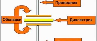
MOSFETs have a very thin layer of insulation between the gate and the channel material. It forms a capacitive coupling between gate-source and gate-drain. Moreover, the dielectric itself creates this effect, working as a capacitance.
We know that any capacitor is manufactured to operate at a certain voltage. If it is exceeded, an insulation breakdown occurs. Ten volts are usually enough to damage the oxide film of the field grass, and sometimes less.
Now I’m showing with photographs what dangers we can create for transistors with our own hands if we don’t follow the rules for soldering them.
I took my favorite Moment transformer soldering iron, plugged its power cord into the outlet, but did not press the power button. I placed one end of the multimeter wire through an alligator clip onto the sting, and the other just leaned it against my finger. Set the AC voltmeter mode.
The device shows 28 volts. This is the kind of interference that is created even when the transformer is de-energized.
I continue the experiment. I left the black probe in the same place, and leaned the red one against the dielectric surface of the stool, where all the instruments are located.
Almost 6.4 volts. When I separated the red probe with air space, the reading became 8 volts.
But these are completely random measurements, the results of which depend on many factors, which means: the voltage can be significantly more or less.
We may not even feel this static, but its random discharge can burn out the thin semiconductor junction of the crystal.
To prevent this, it is important to follow the mandatory recommendations.
How to avoid hidden dangers and work safely with a soldering iron: 5 recommendations
Tip #1: Bypassing the leads
Damage to semiconductor junctions during storage and operation can be prevented by keeping microcircuits, transistors, and integrated electronics products in a layer of foil.
A similar result, in particular, is obtained if you wrap the contacts of their terminals with thin copper wire without insulation.
Tip #2: removing static from operating equipment
It is best to work with a professional soldering station with a grounded tip. If it is not there, then ground the soldering iron tip and the circuit board with separate conductors. Shunt the transistor leads with a thin wire, which will be removed after soldering.
A grounding bracelet on your hand or other part of the body allows you to remove the dangerous potential of static from tweezers and the tool you will be working with. Its 1 MΩ resistance eliminates the possibility of dangerous static discharge.
Tip No. 3: preparing the workplace
The dry air of northern latitudes, especially in winter, contributes to the accumulation of static on surrounding objects. Humidifiers and air washes successfully combat this phenomenon.
An antistatic mat immediately and reliably removes static potentials and the effects of electrical noise from the environment.
Tip #4: professional mixtures
A special flux of the FluxOff brand not only perfectly washes away rosin and traces of corrosion, but actually removes static. They just need to wet the board.
Tip #5: Quick soldering
Choose the minimum required soldering iron power, but work quickly with it. Experienced repairmen manage to heat up the tip, take solder with it, turn off the power to the soldering iron and then solder the part in place.
Some modern microcircuits and transistors are protected against static, but this does not eliminate the need to follow the rules of safe soldering with all other products.
Caution: DC component recovery circuit!
Occasionally, a designer may be faced with a high-voltage circuit that requires isolated gate drive at pulse width ratios around 100%. Previously, the circuit shown in Fig. 1 was recommended for such applications. 6. But its use may damage the power supply when turned off.
Rice. 6. High-voltage circuit with DC component recovery
The diode and capacitor on the secondary side restore the DC component to the gate and provide gate control at relative duration values of up to 90% or more. However, this scheme has a serious drawback, and its use without very careful analysis is not recommended.
This circuit works well in steady state (a load resistor in the gate is recommended), but when the PWM controller is turned off, the coupling capacitor remains connected through the transformer for an indefinite period of time. This can lead to saturation of the transformer, as shown in Fig. 6b. When the transformer saturates, the secondary winding is short-circuited and the capacitor on the secondary side can turn on the DC. Saturation can be prevented by using a gap core and a small capacitor, but this will increase the reactive current required to drive the gate, which causes other problems.
Isolated Gate Control for Bridge Converters
Bridge and half-bridge converters are devices that require a very reliable isolated control circuit. While one of the keys is closed, the key on the other side of the bridge will be open. As a result, a large common mode voltage will be present across the device when it is turned off.
In Fig. Figure 7 shows the circuit recommended for a half-bridge converter. It must be controlled by two transformers. Don't try to use only one transformer and a three-state circuit, as some application manuals advise!
Rice. 7. To drive gates in half-bridge converters, two separate transformers are recommended
In the bridge converter shown in Fig. 8, two transformers are also required to drive the gates. The dual secondary windings in each transformer are used to drive pairs of DCs in the diagonally opposite arms of the bridge. For both types of bridges, gate drive circuits must be carefully tested during turn-on transients, when large peak currents occur and negative gate voltages are low.
Rice. 8. Bridge converter circuit with two transformers to improve reliability
The phase shift bridge circuit (Figure 9) also uses two transformers to drive the gates. But note the difference: each side of the bridge operates at a fixed relative duration of 50%, which allows the use of one transformer with two secondary windings of opposite polarity. This is one of the few designs where a bipolar gate drive can be used without compromising reliability. But surges that occur during turn-off transients should not cause the transistors to open. Pay attention to the polarity of the secondary windings.
Rice. 9. Phase shift bridge with bidirectional transformers in each arm
Conclusion
The gate drive circuit is a critical part of the converter design. Make sure you are using the correct diagram and do not blindly copy diagrams from the application manual. Gate drive transformers give your design a degree of reliability that is not possible with solid-state solutions. If you are developing a very powerful device, then this is a critical component. Adding active elements to conventionally increase switching speed usually does not improve overall performance, but introduces new possibilities for potential failures. Keep your gate control circuit as simple as possible.
Literature
- Balogh L. Design and Application Guide for High Speed MOSFET Gate Drive Circuits. Texas Instruments Application Note.
- Ridley R. Six Reasons for Power Supply Instability. www.switchingpowermagazine.com
- Ridley R. Power Supply Stress Testing. www.switchingpowermagazine.com
- www.ridleyengineering.com