Principles of operation of field-effect transistors in electronic circuits: simplified information
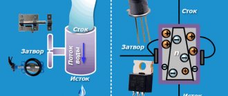
It is convenient to imagine all complex electronic processes using the example of an ordinary water tap with a handle that allows you to turn off the water or regulate its pressure from a very thin trickle (flow) to the strongest possible flow.
I showed this with a primitive picture in which:
- the inlet pipe with pressure is called drain;
- the place of water outlet (outflow) is indicated by the source;
- control handle or valve with a rod - shutter.
The electrical circuit of the field-effect transistor we are considering works in a similar way. Only it has the main constant voltage applied between the drain and source. This area is called a channel. It is made of a semiconductor of a certain structure:
- n-type (electrons predominate - carriers of negative charges);
- p-type - with an excess of positive holes.
In the drawings, these conclusions are shown in one of the following images.
On the shutter designation, we need to pay attention to the direction of the arrow. For n-channel semiconductors it is directed towards the gate, and with p-conductivity it is directed in the opposite direction.
Any field-effect transistors are semiconductors, and controllable ones at that. This means that it passes a load through itself exclusively in one direction, and the opposite movement of electrical charges is always blocked.
The movement of current through semiconductor junctions is always directed from drain to source, just like water in a tap. This is important to remember.
The functions of closing or opening this tap (gate), as well as the role of regulating the force of the flow of electrical charges, are assigned to the gate. Ohm’s well-known law applies here:
I=U/R
The resistance of the channel medium controls the load, and it is acted upon by an externally applied potential.
In other words: the electric field energy applied to the gate changes the resistance of the internal semiconductor junctions and affects the amount of current in the output power circuit.
The word “field” is significant here. It has defined a number of transistor products operating according to this control principle.
The electric field potential controls the amount of resistance across the power semiconductor layer (channel), turning the transistor off/on or changing the current through it.
Bipolar transistors (BTs), about which a previous article was published on my blog, are controlled in a similar way.
Only in them the power circuit is formed between the collector and the emitter, and the control circuit operates from the current generated by the application of voltage between the base and emitter. BT has its own pin designation system, but the same two internal circuits (power circuit and its regulation circuit).
I would like to draw your attention: at the same voltage between the input and output of the field-effect transistor (drain-source), the potential at the gate changes the electrical resistance of the built-in semiconductor junctions.
Moreover, this happens according to one of the scenarios provided in advance. I talk about them successively further.
P-channel serviceability
The serviceability of the p-channel element is checked using the same method as for the n-channel type. The difference is that the red probe must be connected to the minus of the multimeter, and the black wire must be connected to the plus of the device.
Thus, the following conclusions can be drawn regarding field-effect transistor components and test procedures:
- Field elements of the MOSFET variety are widely used in radio electronics, technology and other areas related to practical electronics;
- Checking the performance of transistor elements is most convenient and best done using a multimeter - by following a certain step-by-step method;
- Testing p-channel and n-channel transistor components is carried out using the same methods, but it is necessary to reverse the polarity of the multimeter leads.
Field effect transistor components are very popular in various technical and electronic devices. But for high-quality and durable operation, periodic checking of mosfet transistors using a multimeter is required. By following all the methods described above, you can save significant financial costs associated with replacing and repairing field-effect transistors.
How a field-effect transistor works: 6 types - brief information
The classification shown in the picture below, where their types are structured, will help us deal with a specific field grass and understand its structure.
JFET and MOSFET have different structure. In JFET, the gate (Gate) is directly built into the cross section of the channel and works as a control pn junction.
For mosfet:
- there is an additional fourth pin connected internally to the housing. It is not used when connecting to external circuits;
- The gate output region is separated by a layer of silicon dioxide (dielectric) from the channel semiconductor. It works as a plate capacitively coupled capacitor. Due to this modification, it is called an “insulated gate” or MOS transistor.
MIS stands for metal-dielectric-semiconductor and MOS stands for metal-oxide-semiconductor. The difference between them for a novice electrician is not significant, practically absent.
In the diagrams, mosfet and jifet are designated in different ways. MOSFET is drawn with:
- the fourth pin, which is not connected anywhere;
- a shutter separated from the main channel.
Mosfets are manufactured with different substrates (channels), which can be depleted or enriched in major charge carriers.
I will not describe and describe in more detail the differences between each type of these semiconductors for a novice electrician: there is not much point.
Below are just typical schedules of their work. They will give a general idea of behavior, and you will need to take specific data from the datasheet - technical documentation.
The amount of current flowing through the drain depends on the applied voltage between gate and source, as well as the ambient temperature.
The output drain current characteristics depend on the magnitude of the applied voltage between drain-source and gate-source.
This is how a MOS transistor with a built-in channel works. The current slope increases with increasing voltage Usi, Uzi.
And here are the characteristics of transistors with an induced channel.
Before any check of each transistor, it is necessary to clarify its technical capabilities according to the factory documentation.
Such graphical images and dependencies of electrical engineering processes, due to their clarity, have better information content.
6 features of electronic devices using MOSFETs
Recently, we are increasingly working with mosfet-type field devices with a channel of any conductivity.
Let us briefly analyze such a scheme and its properties.
Point No. 1: which shoulder to place the load on?
When the semiconductor junction is completely open, a very small resistance of tens or hundreds of milliOhms (Ropen) is created between the drain and the source, which forms a low voltage drop in this section (In · Roopen), where In is the value of the load current.
The voltage potential applied to the gate may not be sufficient to fully open the semiconductor. Therefore, the load is turned on higher on the drain side in an n-type field switch, and on the source side in a p-type field switch when the circuit is powered from a single source.
If the device uses additional voltage sources, then this requirement is not necessary.
Point No. 2: tricks for connecting a field worker to microcontrollers
For reliable operation of the MOSFET, it is necessary to apply a threshold voltage value between its gate and source (gate-source), which is indicated in the datasheet. It is usually around 10 volts. Still, digital devices work up to five: their power supply is not enough, you will need to add a level.
You can solve the problem in one of three ways:
- a key with bipolar transistors supplies the necessary power to the gate;
- connect a special driver (chip) to generate a control signal. They are designed for both the upper and lower shoulder to accommodate the load. Moreover, the high-side driver often uses a circuit to increase the output voltage;
- use a specialized low-level field operator (logic level). However, acquiring it can be problematic.
Point No. 3: how to avoid the influence of electrical interference
The appearance of any interference potential at the output of a transistor often leads to its unauthorized switching and disruption of electronic operating algorithms.
Therefore, the gate is always “pulled” to power or ground through a certain resistance, even when connected through a microcontroller. It should not be left in a free state, accessible to the penetration of extraneous interference.
Point No. 4: combating surge current when turned on
The natural presence of capacitance at the gate pin leads to a “current surge” each time the transistor is turned on. This can lead to damage to the semiconductor junction.
The problem is solved by introducing a resistor of sufficient value into the gate circuit. However, its value must be selected taking into account the increase in the key opening time.
Feature No. 5: inrush current protection when disconnecting inductive loads
A protective high-speed TVS diode, connected in parallel between the source and drain, reliably shunts the pulses created by disconnecting inductive loads.
When operating at high frequencies in bridge or half-bridge circuits of switching power supplies or induction heaters of hobs, a Schottky diode is connected counter-currently to the drain output, blocking the parasitic diode, because it increases the closing time, which can damage the semiconductor.
Point No. 6: additional MOSFET
Safe operation of a high-speed high-frequency switch in the switching mode of powerful inductive loads is ensured by its connection to snubber circuits. They:
- aperiodic currents created by transient processes close on themselves;
- reduce heating of semiconductors;
- protect the field switch from unauthorized opening during a rapid increase in voltage between drain and source.
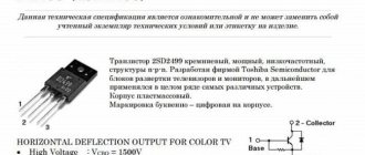
Pinout IRF740
The classic case of the device is TO-220AB. It can withstand severe temperature rises and power dissipation of up to 50W. The pinout is found in most field-effect transistors from this company. The left leg is the gate, the right leg is the source, and the center leg is the drain.
To determine the pinout, you need to take a closer look at the outside of the device with the markings applied to it. When mounting to the board, consider how the case physically connects to the drain pin.
How to solder field-effect transistors correctly and safely: 5 tips
I recommend that beginners pay close attention to this issue. Then you will not be disappointed with the work done.
Where is the ambush hidden or why is static dangerous for electronics?
In everyday life, we rarely feel static electricity, for example, when combing our hair with a plastic comb, getting out of the car after a trip, or in some other cases.
Usually, static causes minor troubles to our body that are simply annoying. But with semiconductors things are different.
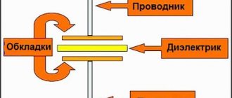
MOSFETs have a very thin layer of insulation between the gate and the channel material. It forms a capacitive coupling between gate-source and gate-drain. Moreover, the dielectric itself creates this effect, working as a capacitance.
We know that any capacitor is manufactured to operate at a certain voltage. If it is exceeded, an insulation breakdown occurs. Ten volts are usually enough to damage the oxide film of the field grass, and sometimes less.
Now I’m showing with photographs what dangers we can create for transistors with our own hands if we don’t follow the rules for soldering them.
I took my favorite Moment transformer soldering iron, plugged its power cord into the outlet, but did not press the power button. I placed one end of the multimeter wire through an alligator clip onto the sting, and the other just leaned it against my finger. Set the AC voltmeter mode.
The device shows 28 volts. This is the kind of interference that is created even when the transformer is de-energized.
I continue the experiment. I left the black probe in the same place, and leaned the red one against the dielectric surface of the stool, where all the instruments are located.
Almost 6.4 volts. When I separated the red probe with air space, the reading became 8 volts.
But these are completely random measurements, the results of which depend on many factors, which means: the voltage can be significantly more or less.
We may not even feel this static, but its random discharge can burn out the thin semiconductor junction of the crystal.
To prevent this, it is important to follow the mandatory recommendations.
How to avoid hidden dangers and work safely with a soldering iron: 5 recommendations
Tip #1: Bypassing the leads
Damage to semiconductor junctions during storage and operation can be prevented by keeping microcircuits, transistors, and integrated electronics products in a layer of foil.
A similar result, in particular, is obtained if you wrap the contacts of their terminals with thin copper wire without insulation.
Tip #2: removing static from operating equipment
It is best to work with a professional soldering station with a grounded tip. If it is not there, then ground the soldering iron tip and the circuit board with separate conductors. Shunt the transistor leads with a thin wire, which will be removed after soldering.
A grounding bracelet on your hand or other part of the body allows you to remove the dangerous potential of static from tweezers and the tool you will be working with. Its 1 MΩ resistance eliminates the possibility of dangerous static discharge.
Tip No. 3: preparing the workplace
The dry air of northern latitudes, especially in winter, contributes to the accumulation of static on surrounding objects. Humidifiers and air washes successfully combat this phenomenon.
An antistatic mat immediately and reliably removes static potentials and the effects of electrical noise from the environment.
Tip #4: professional mixtures
A special flux of the FluxOff brand not only perfectly washes away rosin and traces of corrosion, but actually removes static. They just need to wet the board.
Tip #5: Quick soldering
Choose the minimum required soldering iron power, but work quickly with it. Experienced repairmen manage to heat up the tip, take solder with it, turn off the power to the soldering iron and then solder the part in place.
Some modern microcircuits and transistors are protected against static, but this does not eliminate the need to follow the rules of safe soldering with all other products.
IRF740 Specifications
When studying the characteristics of field workers, you must first take into account its highest possible indicators. Next, following the task, you need to learn about the electrical parameters. Then go to the graphs of typical output transmission values, and others. All this information is contained in the Russian version of DataSheet irf740.
Highs
Let's consider the highest possible performance of the MOSFET IRF740. Do not consider them basic, as if only with them the transistor works normally. Exceeding each of them, even for a short time, can damage the device.
Thermal characteristics
The main parameter limiting the use of a field plant is the temperature required for its normal operation, that is, its increase. It depends on the resistance of the device when electricity passes through it. If it is small, there is still a small amount of power dissipation, which causes heating.
To simplify calculations that depend on the heating of the IRF740, the datasheet contains indicators of its thermal resistance: from the crystal to the case and the crystal to the external environment.
Incorrect thermal calculations for design applications and improper soldering cause overheating of transistors. Once I was reading an amateur radio forum, and one of the participants said that in the circuit he formed, the pirate metal detector was too hot. The electronics engineer took a long time to figure it out, and it turned out that the problem was poor-quality soldering of the device to the board and a decrease in temperature.
IRF740 operating modes
Uzi (voltage) can be either zero or reverse. The second helps to cover the transistor, which is why it is used inside amplifiers of group A and other circuits with smooth regulation.
In the so-called cutoff mode Uzi = Ucutoff. Then it is different for all devices, although it is applied in the opposite direction.
Connection types
By analogy with bipolar speakers, the device in question has 3 connection options:
- With one source. The most common circuit amplifies current and power.
- With one shutter. Unpopular option. Low input voltage, no gain.
- With one drain. The voltage is amplified by almost 100%, the input resistance is high, the output resistance is low. In another way, the circuit is called a current follower.
What can replace IRF740
The device has several foreign analogues:
- D84EQ2 (National Semiconductor).
- STP11NK40Z (STM).
They have outwardly similar bodies and indicators. Therefore, if you include one of these devices in the design diagram, it does not need to be changed. Another similar device suitable for replacement is the Russian analogue of the transistor, KP776. It is manufactured by the Integral company in Belarus. There are several acceptable electrical modes for using this device.
Device details
Matching transformer: W-shaped core, with a cross-sectional area of at least 2 sq.cm. Both windings are wound with PEV-2 wire with a diameter of 0.1 mm. The primary winding consists of 2300 turns, the secondary winding of 644 turns with a tap from the middle of the winding.
When winding, it is advisable to first wind the secondary winding, then insulate it and wind the primary on top of it. You can also use a ready-made miniature transformer from a radio receiver. Usually they come in USH12.5X20 or Sh12X16. Capacitor C1 - K73-5.
The following types of headphones TK-47, TA-56M, TA-4 can be used as an audible alarm.
Source: Homemade electronic devices for the home, Sidorov I.N.
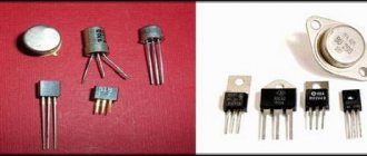
Mosfets - checking, selection of analogues
MOSFET - Metal-Oxide-Semiconductor Field Effect Transistor - MOS field effect transistor.
I’ll add it immediately to the mosfets of the ARM series **** you need to pay close attention
G-GATE S-SOURCE D-DRAIN mosfets are widely used as power transistors for pulsed and linear stabilizer devices, regulating and switching devices. In this topic we will try to clearly explain how to check the mosfets, how to replace them and what to replace them with, as well as collect a minimum of information about analogues and critical replacement, if it turns out even more
1. How to check the mosfet? in order to check it correctly, you need to start by measuring the voltages on them, for this you need to know which mosfet is responsible for what, but measuring the voltage is a completely different topic. very carefully, as they can easily be broken out of the case 2. How to desolder the mosfet? everyone does it differently, personally, I desolder it with a hot-air station or with bottom heating, if the solder is with lead, then I set the temperature to 300 degrees and as soon as the solder floats, I remove the heavier lead-free mosfet with tweezers, I remove it only with bottom heating because I’m afraid of overheating the transistor itself can be desoldered using 2 soldering irons, First, 60 watts, we warm up the base; second, we unsolder the legs and use it to remove the mosfet (personally, I consider this method an unnecessary hassle), some also suggest this option: after warming up the legs, slide a piece of blade under them, and then unsolder the base 3. Having unsoldered the mosfet, we begin to ring for Let's take the most common mosfets in the TO252aa or D2pak housing as a sample
1 leg G-gate, 2 legs or base D-drain, and 3 legs S-source I will show an example of checking on a regular Chinese multimeter EM362
switch the multimeter to diode testing mode and begin to measure the voltage drop for the N-channel mosfet, place the negative (black) probe on the substrate (D-drain), positive (red) on the right terminal of the mosfet (S-source), the tester shows the voltage drop on the internal the diode is about 500 millivolts (readings may be different depending on the mosfets), the field switch is closed, now let’s try to open it, to do this, without lifting the black probe from the substrate, touch the left leg (G-gate) with the red probe, now again move the red probe to the source, the tester shows the voltage drop is equal to 0, (if the tester has a beeper, then it will amuse you with its signature) if you now touch the gate with a black probe and move it back to the substrate, then the mosfet should again show only the voltage drop across the diode; the transistor is closed for the P-channel mosfet to be checked accurately also, only the probes of the device need to be swapped with each other, and if the transistor opened and closed as described here, then rejoice, the mosfet is working, if during the dialing you only touched the transistor with the probes and see 0000 on the tester display, do not worry right away, try to close the mosfet transition first, (this happens quite often) if you find a faulty mosfet, and it is standing and working in tandem with another, then it is advisable to change both transistors (also if you replaced the transistor in one arm with an analogue one, then the second arm must be changed to the same one - same) 4. How to choose an analogue and what to choose? download the datasheet here and select the mosfet according to the parameters. The analog Vds and Vgs should be no less than the original (more is possible), although more precisely they should be greater than the input voltage plus some margin for surges (who knows what margin was already in the original), Id - no less than the original (more is possible), Pd - power dissipation. Rds(on) the lower the better, but if it is a little more than the original, it’s not scary (although it will heat up more). AND YOU MUST NOT FORGET THAT IF YOU INCREASE VDS MUCH, THEN THE OPERATING SPEED OF THE TRANSISTOR WILL BE LOWER, so in pulse circuits we try to select mosfets more precisely about mosfets
about mosfets and analogues
Mosfets in linear stabilizers:
The circuitry is quite popular and simple. An error amplifier on an op-amp, (LM358,324, etc.) or TL431., which controls the gate field switch, opening it (monitoring via feedback), thereby maintaining a constant output voltage. 2.5v, 1.8v, 1.5v, 1.2v, 1.06v.
The mosfet in the linear stabilizer burned out, how to choose an analogue?
In this case, field workers can be divided into 2 groups, differing in the normalized voltage VGS (ON) and the resistance of the open channel RDS (ON). The fact is that designers can optionally power the control circuit on an op-amp from a 12V source as well as from a 5V source. This means that the error amplifier can control the gate field operator from 0 to 9-10V, or from 0 to 4.5-4..8V..
We look at the datasheets, and in some we see normalized RDS (ON) at different VGS (ON).
If the control circuit is 5 volt, you will have to select the transistor more carefully, comparing RDS (ON) & VGS (ON) using datasheets, paying special attention to VGS (ON) = 2.5 V (4.5 V). and RDS (ON) at this voltage. Having compared the “fire victim” with the datasheet, we select it based on characteristics that are no worse than it was. It is possible by selection, but you need to take into account that in an already working circuit there should be no more than 4V on the gate (preferably less) to ensure an adjustment margin.
If it is 12 volt, then almost any mosfet from a donor motherboard (with no less current) will be able to work in this area..
How to determine which scheme is used in a given area.
It’s very simple, without a field operator, by turning on the device, we measure the voltage relative to “ground” at the trigger point in the board. The error amplifier circuit will strive to maximize the voltage at the gate, trying to open the mosfet (which does not exist..
). If we see about 9-10V, then the circuit is 12-volt, the selection parameters are narrowed. If no more than 5V, then the control circuit is 5-volt.