The requirements were as follows: adjustable output voltage up to 30 V with adjustable current limiting up to 5 A. Of course, digital display must be used. The design should resemble MASTECH HY3005D and the like. The only thing is that I never liked that the first device shows current. Well, this is wrong - voltage is always primary, so the first device should show exactly voltage.
Initially, I designed a circuit based on the linear stabilizer K142EN2A, but eventually abandoned this idea - the low efficiency, the regulating power transistor got very hot, even taking into account the fact that a tap switch was provided on the secondary side of the transformer. And in general, everything worked somehow crookedly. I had to cut it out.
The second version of the circuit was developed on the basis of the legendary TL494 PWM controller, which is found in different variations in many computer power supplies. This time everything worked out as it should.
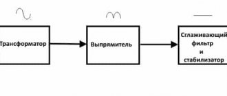
Briefly about the design:
Schematic diagram (clickable)
As I already said, the device was assembled from spare parts, most of which were within a radius of 5 meters from me.
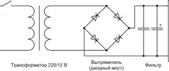
A step-down transformer was found under the table, I don’t know its brand. The voltage on the secondary is about 40 V. D1 - TL494, VD1 - Schottky diode and toroidal choke L1 was removed from a faulty computer power supply: the Schottky diode is used in the rectification circuit, it is installed on the radiator near the pulse transformer, the toroidal choke is located next to it. LM358 is a very good and common operational amplifier. Sold on almost every corner. Recommended for purchase. Shunt R12 - taken from some old communications equipment: it consists of 3 thick bent wires.
Resistors R9, R10 are used to regulate the output voltage (roughly, precisely). Resistors R3, R4 are used to regulate current limiting (rough, fine). When setting up the power supply, trimming resistor R15 adjusts the switching threshold of the LED alarm. There were also problems with the 7805 integrated stabilizer - at an input voltage of about 40 V, it began to glitch terribly - it sank the output voltage, I solved the problem by installing a 1 W quenching resistor R13 at the input.
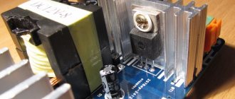
The case itself is taken from an ancient recorder. The layout turned out to be as follows - a power transformer is installed in the middle of the case, which fits in like a native one, apparently they were created for each other. In the front part of the power supply unit there is an electronic control circuit, controls and alarms. The rear of the case houses all the power electronics. Thus, the transformer, as it were, divides the power supply into 2 parts - low-current and power.
The front part of the case with the front cover folded back. Digital measuring instruments came from China, they are factory-made. The electronic control circuit consists of 2 boards: the voltage regulator board - TL494 with wiring, and the alarm board - includes microcircuits D3, D4. Why didn't you do it on one board? I just made the alarm a little later than the regulator, and separately brought it to mind. It also had its problems.
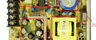
Rear part of the case. A KBPC 3510 diode bridge, a KT827A power transistor, an inductor L1, and a shunt R12 are installed on a common radiator. The whole thing is blown from the inside by a 12 cm fan. The rear of the case also houses fuses, smoothing capacitors C1, C4, and a small auxiliary switching power supply for running the fan and digital meters.
Of course, you could buy a branded power supply and not worry about it. But sometimes you want to reinvent the wheel yourself
If anyone decides to repeat the design, here is a high-resolution schematic diagram and drawings of printed circuit boards in Sprint Layout format.
As time passed, users shared their modifications of power supplies in the comments. Let's take a closer look at the proposed options. Discussion of all designs is still available in the comments
Suggested by acxat_smr
The field driver driver (more precisely, two in parallel - the field workers themselves are responsible for equalizing the currents) is powered from a separate 15V source. I took a 9-36v/15v pro-machinet TEN 12-2413. Coolers are powered from it. TL494 is powered from a separate 24 V source. Any voltage potentiometer, current measurement from an ammeter shunt. The transformer produces 34 V, rectified about 45. The power problem rested on the inductor. If the 5-amp went fine, then the 20 tormented me. In practical terms, I found option two in parallel on the rings from the computer. 23 turns of 1.15mm wire.
Appearance of the structure
Suggested by rond_60
I recently came across this article about LBP on TL494. I was eager to assemble a power supply according to this scheme, especially since a transformer from a Polish power supply for 24V and 4A had been lying around for a long time. The secondary produces 34V alternations, after the bridge with a 10000x63V condenser - 42V. I assembled it using a hinged installation according to this scheme, turned it on and immediately smoke came out of the 494th. I checked everything, replaced the microcircuit, turned it on - it works at idle, the output voltage is trying to regulate, I touched 494 - it’s hot! I added a value of 4.7k to resistor R1 - the unit works, but as soon as I connected a 24V 21W light bulb, the microcircuit exploded in the region of legs 9 and 10. I unwinded several turns from the secondary winding of the trans-ra (reduced the voltage by 4 volts) and the microcircuits still burned. I supplied power to legs 8,11,12 with 12V from another power supply, wound the inductor with wires of different diameters and number of turns - to no avail (I burned 6 microcircuits). I have some experience in converting computer units into chargers and regulated power supplies based on the TL494 and its analogues. I started assembling the PWM harness according to the circuits for computer power supplies. I changed the control of the power transistor, supplied power to the PWM from a separate 12V source (changed the charging from a cell phone) and that’s it - the unit started working! I spent a couple of days setting up adjustments and throttle whistling (no oscillation), now I need to remove the control board and can be assembled into the housing.
Today I set up my PSU. Thank you very much shc68
for the tip, check the ripple at the output with a speaker if you don’t have an oscilloscope.
At low load (bulb 12V, 21W), a hum and howl was heard from the speaker when the current regulator was turned. I eliminated this disgrace by installing additional capacitors (circled in red in the diagram). shc68
recommended, capacitor C15 is really vital. Using the speaker, I also identified a defective potentiometer for current regulation. When it rotated, a rustling and crackling sound was heard from the speaker. After replacing it and installing additional capacitors from the speaker - silence (barely audible hissing) at different loads at the output of the power supply unit. I did a heating test on the block parts. Under such a load, for 1.5 hours only the transistor warmed up (I touched its body with my finger), and the radiator where it was installed was slightly warm (it was blown by a fan). The choke is cold, and so is the transformer.
Laboratory power supply on K143ENZ
My working “laboratory” power supply has been in service for over 20 years. Having repeatedly repaired it after extreme loads, I came to the conclusion that adjustable current protection was necessary. About 5 years ago I developed a power supply circuit based on the K142ENZA chip, and since then I forgot about repairing it. The proposed power supply circuit can serve as both a laboratory voltage source with voltage regulation limits of 3.30 V, and a charger with regulation of the battery charge current.
Fig.1. Schematic diagram of power supply
Stabilizer on K142EN5 - with adjustable output voltage
Design and operating features
- Various personal computers (stationary, with a built-in unit, and laptops, tablets, netbooks, pocket PCs);
- Gadgets (smartphones, audio and video players, cell phones, video cameras and other devices that have a battery in their design);
- Hand-held portable power tools (screwdrivers, grinders, drills, blowers, etc.);
- Various other devices designed for low voltage, capable of operating without being connected directly to a household electrical outlet (LED lamps, shavers, car radios, radios)
Stabilizer on K142EN5 - with adjustable output voltage
In S. Savin’s note “Option for switching on the K142EN5 stabilizer”, published in “Radio” 1989, No. 12, p. 66, it was said that if pin 8 of this microcircuit is connected to the common wire through a zener diode, then the voltage at the output of the stabilizer will increase to the stabilization voltage of the switched on zener diode. Similar advice was repeated by A. Gvozdak in the article “Refinement of the radio designer “Junior-1”,” published in “Radio” No. 6, p. 81-83 for 1991. Experience shows that by selecting the appropriate zener diode it is possible to increase the output voltage of the stabilizer to the required extent, but it, as with the traditional connection of the K142VN5 stabilizer, is fixed. At the same time, readers of our magazine report that a similar method of connecting K142EN5 microcircuit stabilizers allows one to obtain an increased regulated voltage at the stabilizer output. In particular, radio amateurs A. Chumakov from Yoshkar-Ola and A. Cherkasov from Karaganda talk about this in their letters.
Selecting a connection scheme
Current stabilizer on a transistor
In practice, different engineering solutions are used. In particular, manufacturers offer switching power supplies to connect LED lamps. These devices perform their functions using frequency conversion and signal modulation. Microchips are installed to control the key. A throttle is used for measured energy storage.
Pulse current stabilizer
For simplicity, this article considers linear stabilization. Devices created according to this scheme do not create strong electromagnetic interference. This is the main difference from pulse analogues.
STABILIZED POWER SUPPLY
A. POGORELSKY, village. Poikovsky, Tyumen region.
The described power supply is assembled from available elements. It requires almost no setup, operates over a wide range of supplied alternating voltage, and is equipped with overcurrent protection.
The proposed power supply allows you to obtain a stabilized output voltage from 1 V almost to the value of the rectified voltage from the secondary winding of the transformer (see diagram). A comparison unit is assembled on transistor VT1: from the variable resistor R3 motor, part of the reference voltage is supplied to the base (set by the reference voltage source VD5VD6HL1 R1), and the output voltage from the divider R14R15 is supplied to the emitter. The mismatch signal is sent to a current amplifier made on transistor VT2, which controls the control transistor VT4.
When there is a short circuit at the output of the power supply or excessive load current, the voltage drop across resistor R8 increases. Transistor VT3 opens and bypasses the base circuit of transistor VT2, thereby limiting the load current. The HL2 LED signals that overflow protection is turned on.
Do-it-yourself powerful laboratory power supply with a MOSFET transistor at the output
In the previous article, we looked at memory circuits using powerful pnp or npn transistors as a power switch. They made it possible to obtain a fairly large current with a small number of radio components, but the bipolar transistors used have a significant drawback...
- this is a large collector-emitter voltage drop in saturation mode, reaching 2 ... 2.5 V for composite transistors, which leads to their increased heating and the need to install the transistors on a large radiator.
It is much more economical to install power MOS transistors (MOSFETs) instead of bipolar transistors, which at the same currents have a much lower (5-10 times) voltage drop across the open drain-source junction. The easiest way is to install a powerful p-channel field-effect transistor instead of a power PNP transistor, limiting the voltage between the source and gate at 15V using an additional zener diode. A resistor with a resistance of about 1 kOhm is connected in parallel to the zener diode to quickly discharge the gate-source capacitance.
Power n-channel MOS transistors are much more common and accessible, but the circuit diagram of a device with such transistors is somewhat more complicated, because To fully open the drain-source channel, it is necessary to apply a voltage to the gate 15 V higher than the voltage of the power section. Below is a diagram of such a device.
Powerful laboratory power supply 1.5 -30V, 0-5A on a MOSFET transistor
The basis of the design differs little from the previously discussed devices based on bipolar power transistors. Using capacitors C1-C3 and diodes VD1-VD5, a voltage increased by 15 V is formed in the circuit, which is supplied to the gate of field-effect transistor VT1 using transistors VT2, VT3.
In the circuit, it is desirable to use MOSFETs with the lowest open-channel resistance, but the maximum permissible voltage of these transistors should be 1.5 - 2 times higher than the voltage of the power circuit. As a VD8 diode, it is advisable to use diodes with a Schottky barrier with an operating voltage higher than the maximum in the power circuit; in extreme cases, you can use KD213A or KD2997, KD2799, but they will have to be installed on a small radiator. The requirements for the manufacture of storage choke DR1 are the same as for chargers with bipolar key transistors.
In the absence of a suitable wire resistor used as a current shunt R17, the circuit can be modified using a small piece of manganin wire with a diameter of 2 mm or powerful wire resistors with a resistance of 0.01 ... 0.05 Ohm.
The following circuit normalizes the voltage on the current shunt and the amplifier on the op-amp.
Laboratory power supply with shunt voltage normalizer amplifier
The proposed circuit differs from the one described above in the presence of an operational amplifier DA2, which allows you to use either any wirewound resistor with a resistance of 0.01 ... 0.05 Ohm and a power of 1 - 2 W, or a piece of suitable nichrome or manganin wire with a diameter of 1.5 ... 2 mm.
The operational amplifier amplifies the shunt voltage to the level necessary for normal operation of the comparator of the DA1 chip. The gain of op-amp DA2 is determined by the ratio of the resistances of resistors R15 and R18 and is determined from the condition of obtaining a voltage of 0.5 ... 3 V at the output of the op-amp at the selected maximum output current of the device.
The output current is regulated by variable resistor R4, the maximum voltage on the motor of which should be equal to the voltage at the output of op-amp DA2 at the maximum operating current. The resistance of variable resistor R4 can be anything within 1 ... 100 K, and the maximum voltage on its motor is determined by the resistance of resistor R6.
The circuit allows you to obtain a much higher output current than that chosen by the author - the maximum current value is determined by the power of the power transformer, the elements of the power circuit and the setting of the output current limiting unit. Almost any available operational amplifier can be used as DA2, for example KR140UD1408, KR140UD608, KR140UD708, mA741, etc.
Frequency equalization capacitor C9 may be missing when using op amps that do not require its use. In the case of using an op-amp type KR140UD1408 (LM308), it is soldered between pins 1 and 8; for other op-amps, the pins may be different.
Operation of current stabilizers
Transistor voltage stabilizer
The minimum number of functional elements in circuits in this category implies a reasonable cost. When choosing this option, it is not difficult to study the operating modes and configuration features.
Features of field structures
In radio devices of this type, pn junctions are located in a special way. To regulate the passage of current through the central channel, the voltage and the corresponding electromagnetic field are changed. A potential difference is created at the drain and gate.
Operating principle of field-effect and bipolar transistors
The figure shows the fundamental differences compared to a bipolar transistor. When using a field structure, there is no control current, and the input resistance becomes significantly higher. With this scheme, the device consumes a minimum of energy, but is not able to provide signal amplification. However, to solve the indicated problem (stabilization), there is no need to increase the voltage.
Transition control principle
A channel is formed in the area between p-type zones. For the passage of current, a potential difference “drain-source” is created. The transition is controlled by changing the gate-source voltage – Uzi.
DIY 24 Volt voltage stabilizer
The key design elements of voltage stabilizers are:
- transformer;
- resistors;
- capacitors;
- connecting cables for connecting to the network and connecting functional elements;
- active elements.
The operating principle of the simplest stabilizer is based on the operation of a rheostat, which allows you to adjust the circuit resistance depending on the current load. The functionality of such equipment depends on the capabilities of the control systems and the design features of the model, which ideally will completely protect the equipment from network instability.
Among the most effective stabilizing devices are triac units, so we will consider the issue of its manufacture. But initially it is worth taking into account that with your own hands it is only possible to manufacture a device that will be able to effectively equalize the current, but on condition that the range of maximum permissible values for the input voltage and power of the connected electrical receivers is observed. The load switching time will be 10 ms. The list of necessary tools in this case is limited to a soldering iron and tweezers.
Electromechanical (servo-drive) devices
If it is elevated, it moves down. The role of the current collector slider in stabilizers is performed by graphite brushes. They maintain the output voltage with high accuracy (up to 2%), and its adjustment is smooth. These are their main advantages. Some stabilizers, for example, those produced, use not one, but two graphite brushes. This increases the contact area. This device regulates voltage faster.
Some electromechanical models with a power of over 30 kW can be equipped with an additional transformer. Despite the presence of moving parts, devices of this type operate silently. They have a high overload capacity.
By choosing this equipment, you can significantly simplify the calculation: add a quarter of it to the obtained average power of the equipment and thus obtain the characteristics of the future stabilizer. This means that it is permissible to take the minimum reserve of stabilizer power and pay a lower purchase price.
| Manufacturer | power, kWt | Input voltage, W |
| Resanta | 0,5-100 | 140-260240-430 (three-phase) |
| Elitech | 0,5-30 | 160-250280-430 |
| Caliber | 0,5-30 | 160-250 |
| Sturm | 0,5-30 | 140-250 |
The mains voltage is adjusted using a slider that moves along the winding. At the same time, different numbers of turns are used. We all studied at school, and some of us may have dealt with a rheostat in physics lessons.
An electromechanical voltage stabilizer works on this similar principle. Only the slider is moved not manually, but using an electric motor called a servo drive. It is simply necessary to know the structure of these devices if you want to make a 220V voltage stabilizer with your own hands according to the diagram.
Electromechanical devices are highly reliable and provide smooth voltage regulation. Characteristic advantages:
- Stabilizers work under any load.
- The resource is significantly greater than that of other analogues.
- Affordable cost (half lower than electronic devices)
Unfortunately, with all the advantages there are also disadvantages:
- Due to the mechanical design, the response delay is very noticeable.
- Such devices use carbon contacts, which are subject to natural wear and tear over time.
- The presence of noise during operation, although it is practically inaudible.
- Small operating range 140-260 V.
The current is adjusted by connecting more turns of the transformer. In case the device does not have time to react in a timely manner to excessive voltage, a relay is provided in the stabilizer device.
A stabilizer made independently has its pros and cons, which you should definitely know about. Main advantages:
- low cost;
- maintainability;
- independent diagnostics.
The most obvious advantage is its low cost. All parts will need to be purchased separately, and this is still incomparable with ready-made stabilizers.
If any element of the purchased voltage stabilizer fails, it is unlikely that you can replace it yourself. In this case, all that remains is to call a technician to your home or take him to a service center. Even if you have some knowledge in the field of electrical engineering, finding the right part is not so easy. It’s a completely different matter if the device was made by hand. All the details are already familiar and to buy a new one, just visit the store.
If anyone has previously assembled a 220V 10kW voltage stabilizer circuit with their own hands, it means that the person already understands many of the intricacies. This means that identifying the malfunction will not be difficult.