Checking the input resistance
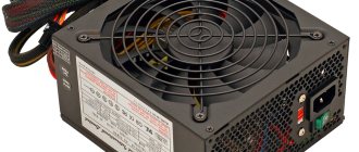
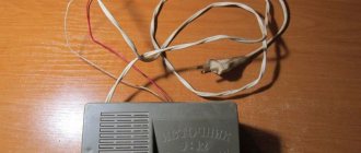
So, they gave us a 350-watt Power Man power supply for repair.
What do we do first? External and internal inspection. Let's look at the "offal". Are there any burnt radio elements? Maybe the board is charred somewhere, or a capacitor has exploded, or it smells like burnt silicon? We take all this into account during the inspection. Be sure to look at the fuse. If it burns out, then replace it with a temporary jumper for about the same amount of Amperes, and then measure the input resistance through two network wires. This can be done on the power supply plug with the “ON” button turned on. It should NOT be too small, otherwise, when you turn on the power supply, a short circuit will occur again.
PSU load
It is necessary to warn that switching on switching power supplies without load significantly reduces their service life and can even cause failure. Therefore, we recommend assembling a simple load block; its diagram is shown in the figure.
Load block diagram
It is advisable to assemble the circuit using resistors of the PEV-10 brand, their ratings are: R1 - 10 Ohms, R2 and R3 - 3.3 Ohms, R4 and R5 - 1.2 Ohms. Cooling for the resistances can be made from aluminum channel.
It is not advisable to connect a motherboard or, as some “craftsmen” advise, a HDD and CD drive as a load during diagnostics, since a faulty power supply can damage them.
We measure voltages
If everything is OK, we turn on our power supply to the network using the network cable that comes with the power supply, and do not forget about the power button if you had it off.
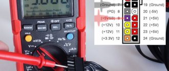
Next, measure the voltage on the purple wire
My patient showed 0 volts on the purple wire. I take a multimeter and connect the purple wire to ground. Ground is black wires with the inscription COM. COM is short for “common,” which means “general.” There are also some types of "lands":
As soon as I touched the ground and the purple wire, my multimeter made a meticulous “ppiiiiiiiiiiiiiiiiiiiiiiiiiiiiiiight” sound and showed zeros on the display. Short circuit, definitely.
Well, let's look for a circuit for this power supply. After googling the Internet, I found a diagram. But I found it only on Power Man 300 Watt. They will still be similar. The only differences in the circuit were the serial numbers of the radio components on the board. If you know how to analyze a printed circuit board for compliance with the circuit, then this will not be a big problem.
And here is the circuit for Power Man 300W. Click on it to enlarge to full size.
We are looking for the culprit
As we see in the diagram, standby power, hereinafter referred to as standby power, is designated as +5VSB:
Directly from it goes a zener diode with a nominal value of 6.3 Volts to the ground. And as you remember, a zener diode is the same diode, but connected in reverse in circuits. The zener diode uses the reverse branch of the current-voltage characteristic. If the zener diode were live, then our +5VSB wire would not short to ground. Most likely the zener diode has burned out and the PN junction is destroyed.
What happens when various radio components burn from a physical point of view? Firstly, their resistance changes. For resistors, it becomes infinite, or in other words, goes into a break. With capacitors it sometimes becomes very small, or in other words, goes into a short circuit. With semiconductors, both of these options are possible, both a short circuit and an open circuit.
In our case, we can check this in only one way, by unsoldering one or both legs of the zener diode, as the most likely culprit of the short circuit. Next, we will check whether the short circuit between the duty switch and ground has disappeared or not. Why is this happening?
Let's remember some simple tips:
1) When connected in series, the rule of greater than greater works, in other words, the total resistance of the circuit is greater than the resistance of the larger resistor.
2) With a parallel connection, the opposite rule works, less than the smaller, in other words, the final resistance will be less than the resistance of the resistor of the smaller value.
You can take arbitrary resistor resistance values, calculate them yourself and see for yourself. Let's try to think logically, if one of the resistances of parallel-connected radio components is zero, what readings will we see on the multimeter screen? That's right, also equal to zero...
And until we eliminate this short circuit by desoldering one of the legs of the part that we consider to be problematic, we will not be able to determine in which part we have a short circuit. The point is that during audio testing, ALL parts connected in parallel to the part that is in a short circuit will ring short with the common wire!
We try to remove the zener diode. As soon as I touched it, it fell apart in two. No comments…
How does the power supply that works in each system unit work?
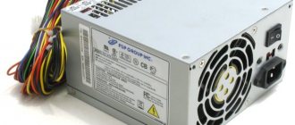
The power supply has been removed from the case.
The bundle of wires on the left connects to the computer. The big component in the middle of the transformer type is the filter inductor. Clickable, like all the photos in the article Have you ever wondered what is inside the power supply unit (PSU) of your computer? The task of the PSU is to convert power from the mains (120 or 240 V alternating current, AC) into a stable supply of direct current, that is, unidirectional current (DC), which your computer needs. The power supply must be compact and cheap, while converting current efficiently and safely. For these purposes, various manufacturing methods are used, and the power supply units themselves are much more complicated inside than you think.
In this article we will analyze the ATX standard unit and explain how it works1. Like most modern power supplies, ours uses a design known as a “switching mode power supply” (UPS). Now they are very cheap, but this was not always the case. In the 1950s, complex and expensive UPS systems were used only in rockets and space satellites with critical size and weight requirements. However, by the early 1970s, new high-voltage transistors and other technological improvements made UPSs much cheaper, so that they became widely used in computers. Today you can buy a phone charger with a UPS inside for a few dollars.
Our ATX UPS is packaged in a metal case the size of a brick, from which comes a multitude of multi-colored cables. Inside the case we see tightly packed components. The design engineers were clearly concerned about the compactness of the device. Many components are covered with radiators. They cool power semiconductors. The built-in fan does the same for the entire power supply. On the KDPV it is on the right.
Let's start with a brief overview of how a UPS works and then describe the components in detail. A kind of “conveyor” in the photograph is organized from right to left. On the right, the UPS receives AC power. The input AC current is converted to high voltage DC using several large filter components. This direct current switches on and off thousands of times per second to generate pulses that are fed into a transformer. It converts high-voltage pulses into high-current low-voltage ones. These pulses are converted to DC and filtered to provide good, clean power. It is supplied to the motherboard, drives and drives through the cables in the photo on the left.
While the process may seem overly complicated, most consumer electronics from cell phones to TVs are actually powered by a UPS. High-frequency current allows you to make a small, lightweight transformer. In addition, pulse power supplies are very effective. The pulses are adjusted to provide only the power needed, rather than turning excess power into waste heat, as in a linear power supply.
The first step is for the input AC current to pass through an input filter circuit, which filters out electrical noise, which is random changes in electrical current that degrade signal quality.
The filter below consists of inductors (toroidal coils) and capacitors. Square gray capacitors are special Class X components for safe connection to AC power lines.
Input Filter Components
Alternating current with a frequency of 60 hertz in the network changes direction 60 times per second (AC), but the computer needs direct current in one direction (DC). The full bridge rectifier in the photo below converts alternating current to direct current. The DC outputs on the rectifier are marked with ? and +, and alternating current enters through two central contacts, which constantly change their polarity. There are four diodes inside the rectifier. The diode allows current to flow in one direction and blocks it in the other direction, so the result is that alternating current is converted to direct current flowing in the desired direction.
The marking GBU606 is visible on the bridge rectifier. The filter circuit is located to the left of the rectifier. The large black capacitor on the right is one of the voltage doublers. The little yellow capacitor is a special ceramic Y-capacitor that protects against voltage surges
Below are two diagrams of how a bridge rectifier works. In the first diagram, the top AC input has positive polarity. The diodes pass current to the DC output. In the second diagram, the AC inputs have changed polarity, as happens all the time in AC. However, the diode configuration ensures that the output current remains unchanged (the plus is always on top). Capacitors smooth the output.
The two diagrams show the current flow as the AC input signal fluctuates. Four diodes cause current to flow in the direction of the arrow
Modern power supplies accept a “universal” input voltage from 85 to 264 volts AC, so they can be used in different countries regardless of the local network voltage. However, the circuitry of this old PSU could not cope with such a wide range. Therefore, a switch is provided to select 115 or 230 V.
Switch 115/230V
The switch uses a clever voltage doubler circuit. The idea is that with the switch closed (at 115V), the AC input bypasses the two bottom diodes in the bridge rectifier and instead connects directly to the two capacitors. When the top AC input is positive, the top capacitor receives full voltage. And when the “plus” is below, then the bottom. Since the DC output comes from both capacitors, the output always produces double the voltage. The fact is that the rest of the power supply receives the same voltage regardless of whether the input is 115 or 230 V, which simplifies its design. The disadvantage of a doubler is that the user must set the switch to the correct position, otherwise they risk damaging the power supply, and the power supply itself requires two large capacitors. Therefore, in modern power supplies, the voltage doubler has gone out of fashion.
Voltage doubler circuit. Each capacitor receives full voltage, so the DC output is double voltage. Gray diodes are not used in doubler operation
For safety reasons, high voltage and low voltage components are separated mechanically and electrically, see photo below.
The main side contains all the circuits that connect to the AC network. On the secondary side there are low voltage circuits. The two sides are separated by "border isolation", which is marked with a green dotted line in the photo. no
across the border . Transformers pass energy across this boundary through magnetic fields without a direct electrical connection. Feedback signals are transmitted to the main side using opto-isolators, that is, light pulses. This separation is a key factor in safe design: a direct electrical connection between the AC line and the PSU output creates a shock hazard.
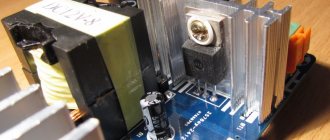
Power supply with markings of main elements. Heatsinks, capacitors, control board and output cables have been removed for better visibility (SB stands for standby supply)
At this point, the input AC current has been converted to high-voltage DC current of about 320 V2. The direct current is cut into pulses by a switching transistor (switching transistor in the diagram above). This is a power MOSFET3. Since it gets hot during use, it is mounted on a large radiator. The pulses are fed into the main transformer, which in a sense is the heart of the power supply.
A transformer consists of several coils of wire wound around a magnetizable core. High-voltage pulses entering the primary winding of the transformer create a magnetic field. The core directs this magnetic field to other, secondary windings, creating voltage in them. This is how the UPS safely produces output current: there is no electrical connection between the two sides of the transformer, only a connection through a magnetic field. Another important aspect is that in the primary winding there are many turns of wire around the core, and in the secondary circuits there are much fewer. The result is a step-down transformer: the output voltage is much less than the input, but at a much higher voltage.
Switching transistor3 is controlled by an integrated circuit called “UC3842B PWM Current Mode Controller”. This chip can be considered the brain of the power supply. It generates pulses at a high frequency of 250 kilohertz. The width of each pulse is adjusted to provide the required output voltage: if the voltage starts to drop, the chip produces wider pulses to pass more energy through the transformer4.
Now you can look at the second, low-voltage part of the power supply. The secondary circuit produces four output voltages: 5, 12, ?12 and 3.3 volts. For each output voltage there is a separate transformer winding and a separate circuit for obtaining this current. Power diodes (below) convert the transformer outputs to DC current. Inductors and capacitors then filter the output from voltage spikes. The power supply must regulate the output voltage to maintain it at the proper level even when the load increases or decreases. Interestingly, BP uses several different control methods.
Close-up view of the output diodes. On the left are cylindrical diodes mounted vertically. In the center are pairs of rectangular Schottky power diodes, with two diodes in each housing. These diodes are attached to a heatsink for cooling. On the right, notice the two copper wires in the shape of staples. They are used as resistors to measure current
The main outputs are 5 and 12 V. They are regulated by a single controller chip on the main side. If the voltage is too low, the IC increases the pulse width, passing more power through the transformer and increasing the voltage on the secondary side of the power supply. And if the voltage is too high, the chip reduces the pulse width. Note: The same feedback circuit drives the 5V and 12V outputs, so a load on one output may change the voltage on the other. In higher quality power supplies, the two outputs are regulated separately5.
Bottom side of the PCB. Pay attention to the large distance between the circuits of the main and secondary sides of the power supply unit. Also note how wide the metal tracks are on the main side of the power supply for high voltage current and how thin the tracks are for control circuits
You may be wondering how the controller IC on the primary side gets feedback about the voltage levels on the secondary side since there is no electrical connection between them (there is a wide gap visible in the photo). The trick is to use a clever chip called an opto-isolator. Inside the chip, on one side of the chip there is an infrared LED, on the other there is a light-sensitive phototransistor. The feedback signal is applied to the LED and detected by a phototransistor on the other side. In this way, the opto-isolator provides a bridge between the secondary and primary sides, transmitting information with light rather than electricity6.
The power supply also provides a negative output voltage (?12 V). This voltage is mostly obsolete, but was used to power serial ports and PCI slots. Regulation of the ?12V supply is fundamentally different from regulation of +5 and +12V. The ?12V output is controlled by a Zener diode (Zener diode), a special type of diode that blocks reverse current until a certain voltage level, and then begins to conduct it. Excess voltage is dissipated as heat through the power resistor (pink) under the control of the transistor and zener diode (since this approach wastes energy, modern high-efficiency power supplies do not use this method of regulation).
The ?12V supply is regulated by a tiny ZD6 zener diode, about 3.6mm long, on the underside of the PCB. The corresponding power resistor and transistor A1015 are located on the top side of the board
Perhaps the most interesting regulation circuit is the 3.3V output, which is regulated by a magnetic amplifier. A magnetic amplifier is an inductor with special magnetic properties that make it work like a key (switch). When current is applied to the inductor of a magnetic amplifier, it initially blocks the current almost completely as the inductor becomes magnetized and the magnetic field increases. When the inductor reaches full magnetization (that is, saturation), its behavior suddenly changes - and the inductor allows particles to flow unimpeded. The magnetic amplifier in the power supply receives pulses from the transformer. The inductor blocks the variable part of the pulse. The 3.3V output is adjusted by changing the pulse width7.
The magnetic amplifier is a ring made of ferrite material with special magnetic properties. Several turns of wire are wound around the ring
The power supply contains a small board on which the control circuit is located. This board compares the voltage with a reference to generate feedback signals. It also monitors voltage to generate a “power good” signal. The circuit is installed on a separate perpendicular board, so it does not take up much space in the power supply.
The main components are mounted on the top side of the board with through-holes, and the bottom side is covered with tiny SMD components that are surface mount. Note the zero resistance resistors as jumpers
The power supply also has a second circuit - for backup power9. Even when the computer is formally "turned off", the five-volt backup power supply provides it with 10 W of power for functions that continue to operate: real-time clock, wake-on-LAN function, etc. The backup power circuit is almost an independent power supply: it uses a separate control chip, separate transformer and separate components on the secondary DC side, but the same components on the primary AC side. This system has a much lower power, so there is a smaller transformer in the circuit.
Black and yellow transformers: the backup transformer is on the left and the main transformer is on the right. A microcircuit is installed in front of it to control backup power. The large cylindrical capacitor on the right is the voltage doubler component. The white beads are silicone, which seals the components and holds them in place
An ATX power supply is complex internally, with many components ranging from massive inductors and capacitors to tiny surface-mount components10. However, this complexity makes it possible to produce efficient, small and safe power supplies. For comparison, I once wrote about a power supply from the 1940s that produced only 85 watts of power, but was the size of a suitcase, weighed 50 kg and cost a fortune. Nowadays, with advanced semiconductors, they make much more powerful power supplies for less than $50, and such a device will fit in your hand.
REC-30 power supply for a 1940s Model 19 (US Navy) teletype
I've written about power supplies before, including a history of power supplies in IEEE Spectrum. You might also like our detailed breakdowns of the Macbook charger and iPhone charger.
1 Intel introduced the ATX standard for personal computers in 1995. The ATX standard (with some updates) still defines the motherboard, case, and power supply configuration of most desktop computers. Here we are studying a power supply from 2005, and modern power supplies are more advanced and efficient. The basic principles are the same, but there are some changes. For example, instead of magnetic amplifiers, DC/DC converters are used almost everywhere.
Label on the power supply
The PSU label indicates that it was manufactured by Bestec for the Hewlett-Packard Dx5150 desktop computer. This power supply slightly does not correspond to the ATX format; it is more elongated in length. [return]
2 You may wonder why 230V AC is converted to 320V DC. The reason is that AC voltage is usually measured as RMS voltage, which in a sense averages out the changing waveform. In fact, a 230-volt AC signal has peaks up to 320 volts. The PSU capacitors are charged through the diodes to peak voltage, so the DC current is approximately 320 volts (although it sags a bit during the cycle). [return]
3 The power transistor is a FQA9N90C power MOSFET. It can handle 9 amps and 900 volts. [return]
4 The integrated circuit is powered by a separate winding on a transformer, which provides 34 volts to operate it. There is a chicken and egg problem: the control chip creates pulses for the transformer, but the transformer powers the control chip. The solution is a special trigger circuit with a 100 kΩ resistor between the microcircuit and the high voltage current. It provides a small current to start the chip. As soon as the chip starts sending pulses to the transformer, it is powered by it. [return]
5 The method of using one control loop for two outputs is called cross control. If the load on one output is much higher than the other, the voltages may deviate from their values. Therefore, many power supplies have minimum load requirements on each output. More advanced power supplies use DC/DC converters for all outputs to control voltage accuracy. For more information on cross-regulation, see these two presentations. One of the methods discussed is multi-level arrangement of output windings, as in our power supply. Specifically, the 12-volt output is implemented as a 7-volt output on top of the 5-volt output, resulting in 12 volts. With this configuration, a 10% error (for example) in a 12-volt circuit would be only 0.7 V, not 1.2 V. [return]
6 The opto-isolators are PC817 components that provide 5000 volts of isolation between the sides of the PSU (that is, between the high and low sides). Note the slot in the PCB under the opto-isolators. This is an additional safety measure: it ensures that high voltage current does not pass between the two sides of the opto-isolator along the surface of the printed circuit board, for example, in the presence of contamination or condensation (in particular, the slot increases the creepage distance). [return]
7 The pulse width through the magnetic amplifier is set by a simple control circuit. In the reverse part of each pulse, the inductor is partially demagnetized. The control circuit regulates the demagnetization voltage. Higher voltage increases demagnetization. The inductor then takes longer to remagnetize and thus blocks the input pulse longer. With a shorter pulse in the circuit, the output voltage decreases. Conversely, a lower demagnetization voltage results in less demagnetization, so the input pulse is not blocked for as long. As a result, the output voltage is regulated by changing the demagnetization voltage. Please note that the pulse width in the magnetic amplifier is controlled by the control chip. The magnetic amplifier reduces these pulses as needed while regulating the 3.3V output voltage. [return]
8 The control board contains several chips, including an LM358NA op-amp, a TPS3510P supervisor/reset chip, an LM339N four-channel differential comparator, and an AZ431 precision reference. The supervisor chip is interesting - it is specifically designed for the PSU and controls the output voltage so that it is not too high and not too low. The AZ431 precision reference is a variant of the TL431 reference chip that is often used in PSUs to provide a reference voltage. I already wrote about the TL431. [return]
9 The backup power supply uses a different configuration - a flyback transformer. A control chip A6151 with a switching transistor is installed here, which simplifies the design.
Power supply circuit using A6151. It is taken from the reference book, therefore it is not identical to the diagram of our power supply, although it is close to it
[return]
10 If you want to study detailed diagrams of various ATX format power supplies, I recommend Dan Melnik’s site. It’s surprising how many power supply implementations there are: different topologies (half-bridge or direct), the presence or absence of power factor conversion (PFC), a variety of control, regulation and monitoring systems. Our power supply is quite similar to the direct topology power supply without PFC, at the bottom of that page on Dan's site. [return]
It's not the zener diode
We check whether the short circuit in the duty and ground circuits has been eliminated or not. Indeed, the short circuit has disappeared. I went to the radio store to get a new zener diode and soldered it. I turn on the power supply, and... I see how my new, just purchased zener diode emits magical smoke)...
And then I immediately remembered one of the main rules of a repairman:
If something burns out, first find the reason for it, and only then replace the part with a new one or risk getting another burnt out part.
Cursing to myself, I bite the burnt zener diode with side cutters and turn on the power supply again.
That’s right, the duty is too high: 8.5 Volts. The main question is spinning in my head: “Is the PWM controller still alive, or have I already burned it safely?” I download the datasheet for the microcircuit and see the maximum supply voltage for the PWM controller, equal to 16 Volts. Phew, looks like it should pass...
Power supply load
When testing power supplies, a load must be connected to them.
The fact is that the power supply units are mostly equipped with protection and alarm elements. These circuits tell the controller that there is no load. It can stop the inverter by reducing the output voltages to zero.
In cheap models, these circuits may be simplified or absent altogether, and therefore the power supply may fail.
When starting the power supply, it is enough to connect a load in the form of wire resistors PEV-25 6 -10 Ohms (to the +12 V bus) and 2 - 3 Ohms (to the +5 V bus).
True, there may be cases when the power supply starts up with such a load, but not with a real load.
But this rarely happens, and again, this is a difficult case. To be honest, you need to load it harder, including the +3.3 V bus.
After repair, it is necessary to check the voltages +3.3 V, +5 V, +12 V. They must be within the tolerance limits - plus or minus 5%. On the other hand, +12V +5% is 12.6V, which is a bit too much...
This voltage is supplied to the drive motors, including the hard drive spindle, which already gets quite hot. If there is regulation, it is better to reduce the voltage to +12 V. However, in inexpensive models there is usually no regulation.
Checking the capacitors
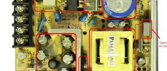
I start googling about my problem on special sites dedicated to repairing ATX power supplies. And of course, the problem of overestimated standby voltage turns out to be a banal increase in the ESR of electrolytic capacitors in the standby circuits. We look for these capacitors in the diagram and check them.
I remember my assembled ESR meter
It's time to check what he is capable of.
I check the first capacitor in the duty circuit.
ESR is within normal limits.
Finding the culprit of the problem
I'm checking the second one
I wait for a value to appear on the multimeter screen, but nothing has changed.
I understand that the culprit, or at least one of the culprits of the problem, has been found. I resolder the capacitor to exactly the same one, in terms of nominal value and operating voltage, taken from the donor power supply board. I want to go into more detail here:
If you decide to put an electrolytic capacitor into an ATX power supply not from a donor, but a new one from a store, be sure to buy LOW ESR capacitors and not regular ones. Conventional capacitors do not work well in high-frequency circuits, but in the power supply, these are precisely the circuits.
So, I turn on the power supply and measure the voltage at the control room again. Having learned from bitter experience, I am no longer in a hurry to install a new protective zener diode and measure the voltage at the control room, relative to the ground. The voltage is 12 volts and a high-frequency whistle is heard.
Again I sit down to google about the problem of overvoltage in the duty room, and on the rom.by website, dedicated to both the repair of ATX power supplies and motherboards, as well as all computer hardware in general. I find my fault by searching for typical faults of this power supply. It is recommended to replace the capacitor with a capacity of 10 µF.
I measure ESR on the capacitor.... Ass.
The result is the same as in the first case: the device goes off scale. Some say, why collect some devices, such as swollen non-working capacitors, you can see that they are swollen, or have opened like a rose
Yes, I agree with this. But this only applies to large capacitors. Capacitors of relatively small values do not swell. There are no notches in their upper part through which they could open. Therefore, it is simply impossible to determine their performance visually. All that remains is to replace them with ones that are known to work.
So, after going through my boards, I found the second capacitor I needed on one of the donor boards. Just in case, its ESR was measured. It turned out to be normal. After soldering the second capacitor into the board, I turn on the power supply using the key switch and measure the standby voltage. Exactly what was required, 5.02 volts... Hurray!
I measure all other voltages at the power supply connector. Everything corresponds to the norm. Operating voltage deviations are less than 5%. It remains to solder a 6.3 Volt zener diode. I thought for a long time why the zener diode is 6.3 Volts when the voltage on duty is +5 Volts? It would be more logical to set it to 5.5 volts or similar if it was used to stabilize the voltage on the duty room. Most likely, this zener diode is placed here as a protective one, so that if the voltage on the control panel increases above 6.3 Volts, it will burn out and short-circuit the control panel circuit, thereby turning off the power supply and saving our motherboard from burning out when entering over-voltage through the control room.
The second function of this zener diode is, apparently, to protect the PWM controller from receiving too much voltage. Since the control room is connected to the power supply of the microcircuit through a fairly low-resistance resistor, almost the same voltage is supplied to pin 20 of the PWM microcircuit that is present in our control room.
Refinement of power supply
In conclusion, we will give some tips on improving the power supply, which will make its operation more stable:
- in many inexpensive units, manufacturers install two-amp rectifier diodes; they should be replaced with more powerful ones (4-8 amperes);
- Schottky diodes on the +5 and +3.3 volt channels can also be installed more powerful, but they must have an acceptable voltage, the same or greater;
- It is advisable to replace the output electrolytic capacitors with new ones with a capacity of 2200-3300 μF and a rated voltage of at least 25 volts;
- It happens that instead of a diode assembly, diodes soldered together are installed on the +12 volt channel; it is advisable to replace them with a Schottky diode MBR20100 or similar;
- if 1 µF capacitances are installed in the key transistors, replace them with 4.7-10 µF, designed for a voltage of 50 volts.
Such a minor modification will significantly extend the life of the computer power supply.
Very interesting to read:
- DIY power supply for 12V LED strip
- Operating principle of a full-wave rectifier