Relay circuits are used in automatic control systems: to maintain a given temperature, light, humidity, etc. Such circuits are usually similar and contain a sensor, a threshold circuit and an actuator or indicator device as mandatory components (see the list of references).
Relay circuits react to the excess of the controlled parameter above a given (set) level and turn on the actuator (relay, electric motor, one or another device).
It is also possible to notify with a sound or light signal that the controlled parameter has gone beyond the permissible level.
Transistor thermal relay
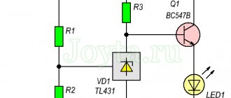
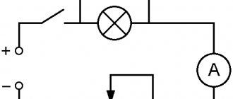
The thermal relay (Fig. 1) is based on a Schmitt trigger. A thermistor (a resistor whose resistance depends on temperature) is used as a temperature sensor.
Potentiometer R1 sets the initial bias on thermistor R2 and potentiometer R3. By adjusting it, the actuator (relay K1) is activated when the resistance of the thermistor changes.
Rice. 1. Scheme of a simple thermal relay using transistors.
Not only a relay, but also a low-current incandescent lamp can be used as a load in this and other circuits in this chapter.
You can turn on an LED with a series current-limiting resistor of 330...620 Ohms, a sound generator, an electronic siren, etc.
When using a relay, the contacts of the latter can include any load electrically isolated from the sensor circuit: a heating element or, conversely, a fan.
To protect the output transistor from voltage pulses that occur when switching the relay winding (inductive load), it is necessary to connect a semiconductor diode in parallel with the relay winding.
So, in Fig. 1 anode of the diode must be connected to the bottom terminal of the relay winding according to the diagram, the cathode - to the power bus. Instead of a diode, a zener diode or capacitor can be connected with the same result.
How a field-effect transistor works: 6 types - brief information
The classification shown in the picture below, where their types are structured, will help us deal with a specific field grass and understand its structure.
JFET and MOSFET have different structure. In JFET, the gate (Gate) is directly built into the cross section of the channel and works as a control pn junction.
For mosfet:
- there is an additional fourth pin connected internally to the housing. It is not used when connecting to external circuits;
- The gate output region is separated by a layer of silicon dioxide (dielectric) from the channel semiconductor. It works as a plate capacitively coupled capacitor. Due to this modification, it is called an “insulated gate” or MOS transistor.
MIS stands for metal-dielectric-semiconductor and MOS stands for metal-oxide-semiconductor. The difference between them for a novice electrician is not significant, practically absent.
In the diagrams, mosfet and jifet are designated in different ways. MOSFET is drawn with:
- the fourth pin, which is not connected anywhere;
- a shutter separated from the main channel.
Mosfets are manufactured with different substrates (channels), which can be depleted or enriched in major charge carriers.
I will not describe and describe in more detail the differences between each type of these semiconductors for a novice electrician: there is not much point.
Below are just typical schedules of their work. They will give a general idea of behavior, and you will need to take specific data from the datasheet - technical documentation.
The amount of current flowing through the drain depends on the applied voltage between gate and source, as well as the ambient temperature.
The output drain current characteristics depend on the magnitude of the applied voltage between drain-source and gate-source.
This is how a MOS transistor with a built-in channel works. The current slope increases with increasing voltage Usi, Uzi.
And here are the characteristics of transistors with an induced channel.
Before any check of each transistor, it is necessary to clarify its technical capabilities according to the factory documentation.
Such graphical images and dependencies of electrical engineering processes, due to their clarity, have better information content.
6 features of electronic devices using MOSFETs
Recently, we are increasingly working with mosfet-type field devices with a channel of any conductivity.
Let us briefly analyze such a scheme and its properties.
Point No. 1: which shoulder to place the load on?
When a semiconductor junction is fully open, a very small resistance of tens or hundreds of milliOhms (Ropen) is created between drain and source, which creates a low voltage drop across
and in this section (In·Ropen), where In is the value of the load current.
The voltage potential applied to the gate may not be sufficient to fully open the semiconductor. Therefore, the load is turned on higher on the drain side in an n-type field switch, and on the source side in a p-type field switch when the circuit is powered from a single source.
If the device uses additional voltage sources, then this requirement is not necessary.
Point No. 2: tricks for connecting a field worker to microcontrollers
For reliable operation of the MOSFET, it is necessary to apply a threshold voltage value between its gate and source (gate-source), which is indicated in the datasheet. It is usually around 10 volts. Still, digital devices work up to five: their power supply is not enough, you will need to add a level.
You can solve the problem in one of three ways:
- a key with bipolar transistors supplies the necessary power to the gate;
- connect a special driver (chip) to generate a control signal. They are designed for both the upper and lower shoulder to accommodate the load. Moreover, the high-side driver often uses a circuit to increase the output voltage;
- use a specialized low-level field operator (logic level). However, acquiring it can be problematic.
Point No. 3: how to avoid the influence of electrical interference
The appearance of any interference potential at the output of a transistor often leads to its unauthorized switching and disruption of electronic operating algorithms.
Therefore, the gate is always “pulled” to power or ground through a certain resistance, even when connected through a microcontroller. It should not be left in a free state, accessible to the penetration of extraneous interference.
We recommend reading: What is a capacitor and why is it needed?
Point No. 4: combating surge current when turned on
The natural presence of capacitance at the gate pin leads to a “current surge” each time the transistor is turned on. This can lead to damage to the semiconductor junction.
The problem is solved by introducing a resistor of sufficient value into the gate circuit. However, its value must be selected taking into account the increase in the key opening time.
Feature No. 5: inrush current protection when disconnecting inductive loads
A protective high-speed TVS diode, connected in parallel between the source and drain, reliably shunts the pulses created by disconnecting inductive loads.
When operating at high frequencies in bridge or half-bridge circuits of switching power supplies or induction heaters of hobs, a Schottky diode is connected counter-currently to the drain output, blocking the parasitic diode, because it increases the closing time, which can damage the semiconductor.
Point No. 6: additional MOSFET protection
Safe operation of a high-speed high-frequency switch in the switching mode of powerful inductive loads is ensured by its connection to snubber circuits. They:
- aperiodic currents created by transient processes close on themselves;
- reduce heating of semiconductors;
- protect the field switch from unauthorized opening during a rapid increase in voltage between drain and source.
Simple temperature indicator
The thermal relay (Fig. 3), or, more precisely, the thermal indicator, is made according to a bridge circuit [VRL 83-24]. When the bridge is balanced, none of the LEDs light up. As soon as the temperature rises, one of the LEDs will turn on.
Rice. 3. Schematic diagram of a simple thermal indicator using one transistor and LEDs.
If the temperature, on the contrary, decreases, another LED will light up. To distinguish in which direction the temperature is changing, you can use a red LED to indicate an increase in temperature, and a yellow (or green) LED to indicate a decrease. To balance the circuit, it is better to include a potentiometer instead of resistor R2.
An example of transistor operation in switch mode
Gain is one of the main characteristics of a transistor. It is this parameter that shows how many times the current flowing through the emitter-collector channel is higher than the base one. Let's say the coefficient is 100 (this parameter is designated h21E). This means that if a current of 1 mA (base current) is supplied to the control circuit, then at the collector-emitter junction it will be 100 mA. Consequently, the incoming current (signal) was amplified.
We recommend reading: Labeling capacitors - capacitor decoding table
During operation, the transistor heats up, so it needs passive or active cooling - radiators and coolers. But heating occurs only when the collector-emitter passage does not open completely. In this case, a lot of power is dissipated - it needs to be put somewhere, you have to “sacrifice” the efficiency and release it in the form of heat. Heating will be minimal only in cases where the transistor is closed or fully open.
Photo relay with two-stage amplifier
Photo relay circuit shown in Fig. 5 contains a two-stage DC amplifier made of transistors of different conductivity types.
Rice. 5. Schematic diagram of a photo relay with a two-stage amplifier.
When the electrical resistance of the photodiode and, accordingly, the bias at the base of the transistor VT1 changes, the collector current of the output transistor of the amplifier VT2 will increase, and the voltage across the resistor R2 will increase.
As soon as this voltage exceeds the breakdown voltage of the threshold element - the semiconductor zener diode VD2, the final stage on the transistor VT3 is turned on, controlling the operation of the actuator (relay).
The use of a threshold element (semiconductor zener diode) in the circuit increases the clarity of the photo relay operation.
Setup procedure 2
To achieve the maximum time delay, the setting current is set from the base bias circuit of transistor VT2 through thyristor VS1 by selecting resistors R8, R9. The current is measured with a milliammeter.
The common point of resistors R8 and R9 is connected to “-” through a diode, which serves to compensate for the correction of the anode-cathode transition of thyristor VS1. By selecting resistors R8 and R9, the operating current is set to a maximum of 2.7...2.9 mA (about 90%) of the total current, but is not brought to the initial shutdown current of the thyristor VS1, otherwise the thyristor may not close due to the base current. Next, resistor R6 of the operating current circuit for supplying the thyristor from the emitter of transistor VT1 of the timing circuit is selected.
This calculation is that when the current through resistor R6 reaches less than 0.42 mA (about 10% of the thyristor holding current), thyristor VS1 will close. Next, we charge capacitor C1. When relay K1 turns on, we close the circuit of capacitor C1, the capacitor will discharge.
Relay K1 should turn off quickly, this should be repeated several times. Note: when using transistors VT2 of other types with low base currents, and especially a transistor of pnp conductivity, when the holding current of the thyristor is more than 8 mA, it is recommended to additionally connect a ballast resistance through the thyristor VS1 according to the diagram in Fig. 4.
Test practice has shown that thyristors KU101E and KU101G have holding currents of 2...5 mA, and KU101A - mostly more than 8 mA. Tests were also carried out on triacs, in particular TS6-10, whose holding current was 5 mA.
The device in Fig. 4 differs from the device in Fig. 3 in that, in addition, the anode of the thyristor VS1 is connected to the power source “+” through a current setter consisting of elements of a trimming resistor R8 and a current-limiting resistor R9. The elements of the current setter are ballast resistors, which are installed at high thyristor holding currents.
Regulator R8 adjusts the thyristor current over a wide range, which also changes the relay dwell time. The main purpose of the setter is to select the setting current (subject to 90% of the holding current) through the thyristor, and the remaining holding current (10%) through the timing chain must be maintained.
Diode VD3 blocks the base of the switch of transistor VT2 from additional communication with “+” through the elements of the current setter. Also, diode VD3 improves the switching dynamics of the switch of transistor VT2.
The second difference between the device (Fig. 4) and the device (Fig. 3) is that the switching unit is installed on a transistor VT2 with pn-p conductivity. Relay K1 will be turned on when the power source is turned on, and when the SB1 button is pressed, relay K1 is turned off for the set delay time. In Fig. Figure 5 shows the device of an electronic relay based on a triac optocoupler U1 type MOS3063 or MOS3082.
The tests have shown that the holding current of these triacs is in the range of 0.4...0.7 mA, and in the description circuit the minimum holding current on the U1 MOS3063 optocoupler was 0.55 mA.
With this connection, galvanic isolation is lost between the control LED and the output of the optocoupler switch, and the operating principle is similar to a triode thyristor switch.
Diode VD4 blocks the base of transistor VT2 from communication with “-” through the optocoupler LED when the optocoupler key is closed, zener diode VD3 is installed to compensate for the voltage drop at the junction of the control LED, i.e. the total voltage drop across the transition increases, which should not be less than the transition circuit of the triac switch. The parameters of zener diodes can be changed to other values.
To open the phototriac key in a direct current source, a short-term operating current pulse on the optocoupler LED is sufficient, and the key switches to diode mode. With the installation of zener diode VD3, when a certain voltage is reached at the emitter of transistor VT1, the current through the optocoupler LED closes, the current will flow only through the high resistance of the optocoupler switch circuit, which increases the relay dwell time.
Capacitor C2 serves for additional pulse activation of triac U1, which is especially necessary when increasing the value of current-limiting resistor R5 and zener diode VD3.
Zener diode VD2 serves to protect the optocoupler LED, the maximum permissible current of which is achieved at a voltage of 1.5 V at the junction of the control LED of the optocoupler key.
This phototriac has a very low holding current, so the transistor output switch circuit is made using a composite transistor VT2 and VT3 with a high input resistance. The principle, setup and operating conditions are similar to the description of a triode thyristor.
With careful selection of elements with a given value of capacitor C1, you can achieve a much longer time delay with the selection of resistors R6 and R8. The holding time in this scheme was 0... 40 minutes.
As the value of resistor R6 increases, the time delay increases, but the error may increase. With repeated testing, the error averaged within 2%.
This error depends not only on the photosimulator itself, but also on the circuit elements. The main advantage of the optocoupler switch on this triac is characterized by a steep characteristic, i.e. the relay coil is instantly switched off from the supply voltage to zero.
Photo relay with sound alarm
The photo relay (Fig. 6) is not fully such, since it responds to changes in illumination by smoothly changing the frequency of the generated oscillations [BC Ivanov].
Rice. 6. Schematic diagram of a photo relay with a sound alarm.
At the same time, this device can work in conjunction with frequency-measuring devices, frequency-selective relays, and signal changes in illumination with the height of the sound signal, which can be very important for the visually impaired.
Humidity relay circuit, liquid level relay
The humidity relay or liquid level relay (Fig. 7), like some of the above circuits, is based on a Schmitt trigger [MK 2/86-22].
Rice. 7. Schematic diagram of a humidity relay, liquid level relay.
The device response threshold is set by adjusting potentiometer R3. The humidity sensor contacts are made in the form of copper (Ci) and iron (Fe) rods immersed in the ground.
When the moisture content in the ground changes, the electrical conductivity of the medium and the resistance between the electrodes change. As the bias at the base of transistor VT1 increases, it opens.
The collector and emitter currents of the transistor increase, which leads to an increase in the voltage on the potentiometer R3 and, accordingly, to switching the trigger.
The relay is activated. The device can be configured to reduce the electrical conductivity of the earth below a specified norm. Then, when the actuator is triggered, the automatic watering system for the soil (plants) is turned on.
What to choose
- Insignificant value of residual voltage on the key in the wiring condition.
- High resistance and, as a result, low current that flows through the closed element.
- Low power consumption means no significant control voltage source is needed.
- It is possible to switch low-level electrical signals that amount to units of microvolts.
A transistor relay switch is an ideal application for field applications. Of course, this message is posted here solely to give readers an idea of their application. With a little knowledge and ingenuity, a great many possibilities for implementations that include transistor switches will be invented.
Time relay
Time relay (Fig. described in the book by P. Velichkov and V. Hristov (Bulgaria). A short press on the SA1 button discharges the time-setting capacitor C1 and the device begins “counting time.”
Rice. 8. Schematic diagram of a time relay using transistors.
As the capacitor charges, the voltage on its plates gradually increases. As a result, after some time the relay will operate and the actuator will turn on.
The charging rate of the capacitor, and therefore the holding time (exposure time), can be changed with potentiometer R1. The relay provides a maximum exposure time of up to 10 seconds with the parameters of the elements indicated on the diagram. This time can be increased by increasing the capacitance of capacitor C1 or the resistance of potentiometer R1.
It is worth noting that for such simple “analog” timer circuits, the stability of the time interval is low. In addition, it is impossible to increase the capacitance of the timing capacitor indefinitely, since its leakage current increases noticeably.
Such a capacitor is unacceptable in “analog” timer circuits. It is also impossible to significantly increase the exposure time due to the resistance of potentiometer R1, since the input resistance of subsequent stages, unless they are made using field-effect transistors, is small.
Analog timers (time relays) are widely used in photo printing to set the time for performing any procedures. These devices are used, for example, to produce silver-ionized water.
A relay that responds to voltage level
Voltage relays (Fig. 9, 10) are used to control the charge or discharge of batteries, batteries, control the supply voltage, and maintain the voltage at a given level. The circuits described in the book by P. Velichkov and V. Hristov are designed to control the discharge (Fig. 9) or overcharge (Fig. 10) of the battery.
Rice. 9. Schematic diagram of a relay for monitoring battery discharge.
Rice. 10. Schematic diagram of a relay for monitoring battery overcharge.
If necessary, the response voltage of these devices can be changed. The response threshold is set by the type of zener diode. To change the operating threshold of such relays within small limits, 1 - 3 germanium Shch9) or silicon (KD503, KD102) diodes can be connected in series with the zener diode in the forward direction.
The cathodes of the diodes should “look” towards the base of the input transistor. A germanium diode shifts the operating threshold by approximately 0.3 V, and a silicon diode by 0.5 V.
For a chain of two or three diodes, these values are doubled (tripled). Intermediate voltage values can be obtained by connecting germanium and silicon diodes in series (0.8 V).