Transistor amplifier
The transistor acts as an amplifier, increasing the strength of a weak signal. A DC bias voltage applied to the base of the emitter junction causes it to remain in the forward biased state. This forward bias is maintained regardless of signal polarity. The figure below shows what a transistor looks like when connected as an amplifier.
The low resistance of the input circuit allows any small change in the input signal to result in a large change in the output signal. The emitter current caused by the input signal introduces a collector current, which, when flowing through the load resistor RL, causes a significant voltage drop across it. Thus, a small input voltage results in a large output voltage, which shows that the transistor is working as an amplifier.
example
Let there be a change in input voltage of 0.1 V, which will additionally change the emitter current by 1 mA. This emitter current will obviously cause a change in collector current, which will also be 1 mA.
A 5k ohm load resistance placed in the collector will produce a voltage
5 kOhm × 1 mA = 5 V
Therefore, it is observed that a change of 0.1 V in the input results in a change of 5 V in the output, which means that the voltage level of the signal is enhanced.
Operation of current stabilizers
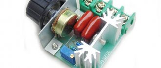
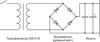
DIY 220V voltage stabilizer circuit
The minimum number of functional elements in circuits in this category implies a reasonable cost. When choosing this option, it is not difficult to study the operating modes and configuration features.
Features of field structures
In radio devices of this type, pn junctions are located in a special way. To regulate the passage of current through the central channel, the voltage and the corresponding electromagnetic field are changed. A potential difference is created at the drain and gate.
The figure shows the fundamental differences compared to a bipolar transistor. When using a field structure, there is no control current, and the input resistance becomes significantly higher. With this scheme, the device consumes a minimum of energy, but is not able to provide signal amplification. However, to solve the indicated problem (stabilization), there is no need to increase the voltage.
Transition control principle
A channel is formed in the area between p-type zones. For the passage of current, a potential difference “drain-source” is created. The transition is controlled by changing the gate-source voltage – Uzi.
Amplifier Performance
Since the general emitter connection type is mostly accepted, let's first understand a few important terms related to this connection mode.
Input impedance
Since the input circuit is forward biased, the input impedance will be low. Input resistance is the resistance created by the base-emitter junction to signal flow.
By definition, it is the ratio of a small change in base-emitter voltage (ΔV BE) to the resulting change in base current (ΔI B) at a constant collector-emitter voltage.
Input resistance, Ri= frac DeltaVBE DeltaIB
Where R i = input resistance, V BE = base-emitter voltage and IB = base current.
Output impedance
The output impedance of the transistor amplifier is very high. The collector current changes very little with changes in the collector-emitter voltage.
By definition, it is the ratio of the change in collector-emitter voltage (ΔV CE) to the resulting change in collector current (ΔI C) at a constant base current.
Output impedance = Ro= frac DeltaVCE DeltaIC
Where R o = output resistance, V CE = collector-emitter voltage and IC = collector-emitter voltage.
Effective load on the collector
The load is connected to the collector of the transistor and for a single stage amplifier the output voltage is taken from the collector of the transistor and for a multi stage amplifier the same is collected from the cascaded stages of the transistor circuit.
By definition, it is the total load seen by the AC collector current. In case of single stage amplifiers, the effective collector load is a parallel combination of RC and R o .
Effective collector load, RAC=RC//Ro
= fracRC timesRoRC+Ro=RAC
Therefore, for a single stage amplifier, the effective load is equal to the collector load R C.
In a multistage amplifier (that is, having more than one amplification stage), the input resistance R i of the next stage is also taken into account.
The effective collector load becomes a parallel combination of RC, R o and R i, i.e.
Effective collector load, RAC=RC//Ro//Ri
RC//Ri= fracRCRiRC+Ri
Since the input resistance R i is quite small, hence the effective load is reduced.
Current profit
The current gain when changes in input and output currents are observed is called current gain
. By definition, it is the ratio of the change in collector current (IC) to the change in base current (IB).
Current profit, beta= frac DeltaIC DeltaIB
The value of β ranges from 20 to 500. The current gain indicates that the input current becomes β times the collector current.
Voltage boost
The voltage gain when changes in input and output currents are observed is called voltage gain
. By definition, it is the ratio of the change in output voltage (ΔV CE) to the change in input voltage (ΔV BE).
Voltage gain, AV= frac DeltaVCE DeltaVBE
= frac Change to output current effective load Change to input current input resistance
= frac DeltaIC timesRAC DeltaIB timesRi= frac DeltaIC DeltaIB times fracRACRi= beta times fracRACRi
For one stage R AC = R C.
However, for multi-stage,
RAC= fracRC timesRiRC+Ri
Where R i is the input resistance of the next stage.
Do-it-yourself powerful electronic load
The maximum input voltage is up to 60V, more is possible, it all depends on the voltage of the transistors.
Also, the electronic load is protected against polarity reversal. Maximum power dissipation is about 1500-1600W
Such a device is capable of loading almost any power source, even welding inverters, but it is important not to exceed the maximum power, and here, as mentioned above, it is 1600 W. It is worth noting that all 1600W in this case will be used for heating, so this is a fairly serious heater
I think you'll agree that the above specifications are truly impressive for a linear load. Current loads with similar parameters are quite expensive, naturally our version will not have any special bells and whistles.
Attention! It’s worth noting a few points right away to avoid additional questions. Firstly, the diagram turned out to be quite large and most likely some small details will not be visible
You will find the diagram in good quality in the project archive. Also, a link to download the archive is in the description under the author’s original video.
Secondly,
The values of some circuit elements may differ from those installed on the board, but the device will work in both cases.
Third,
the most preferred transistors TIP142 were used in the circuit, these are composite switches that are easy to operate and the driver will hardly heat up, but the total load power with the switches indicated in the diagram will be less than in this case, since the transistors used here are much more powerful .
The lower the value of this resistance, the greater the current. The specified resistor must be selected. The author conducted numerous experiments with the resulting device to find out how much power a transistor in such a package can dissipate, the maximum collector current, and how heavily the control driver will be loaded at different current values on the power transistor.
The tests were successful, and not a single transistor was damaged. Through experience, it became clear that the 32A transistors declared by the manufacturer hold up. The case is capable of dissipating 150W, and with a fan, even 200W.
The value of 200W from each transistor, you see, is quite good. And the author screwed 4 keys onto each radiator using thermal paste. In this case there are 2 such radiators.
It is worth noting that the above circuit operates in linear mode, so the transistors are open or partially closed during the process, this depends on the output voltage of the operational amplifier.
The more open the power transistor is, the greater the current in the circuit and vice versa. As mentioned above, all power is released as heat on the power transistors and current sensors, so if you want to repeat this project, first of all take care of good cooling of these circuit components. The author used fairly good aluminum radiators in the form of a bar.
The first variable is used for rough adjustment, the second, respectively, for smoother adjustment. The control board requires a low-power power supply. For example, it can be powered by batteries or accumulators. This solution will make the load completely autonomous.
The power diodes mentioned at the beginning of the article are installed at the load input. They are protected against polarity reversal. The reverse voltage and current of the diode should be selected with a double margin. In the future, the author plans to change the protection to another one, most likely using field-effect transistors.
This is how another monster was born, it’s quite difficult to come up with another name for this beast, horse radiators and power keys, brutal power, what else is needed for complete happiness. That's all for today
Thank you for attention. See you again!
Author's video:
Protection resistors
Every radio amateur is probably familiar with the smell of a burnt resistor. This is the smell of burning varnish, epoxy resin and... money. Meanwhile, a cheap resistor can save your amplifier!
The author, when turning on the amplifier for the first time, installs low-resistance (47-100 Ohms) resistors in the power circuits instead of fuses, which are several times cheaper than fuses. This has more than once saved expensive amplifier elements from installation errors, incorrectly set quiescent current (the regulator was set to maximum instead of minimum), reversed power polarity, and so on.
The photo shows an amplifier where the installer mixed up TIP3055 transistors with TIP2955.
The transistors were not damaged in the end. Everything ended well, but not for the resistors, and the room had to be ventilated.
Analogs LM358
Complete analogs of LM358 from different manufacturers NE532, OP04, OP221, OP290, OP295, OPA2237, TA75358P, UPC358C. For LM358D - KIA358F, NE532D, TA75358CF, UPC358G.
Along with the LM358, a large number of similar operational amplifiers are produced. For example, LM158, LM258, LM2409 have similar characteristics, but different operating temperature ranges.
| Type | Minimum temperature, °C | Maximum temperature, °C | Supply voltage range, V |
| LM158 | -55 | 125 | from 3(±1.5) to 32(±16) |
| LM258 | -25 | 85 | from 3(±1.5) to 32(±16) |
| LM358 | 70 | from 3(±1.5) to 32(±16) | |
| LM358 | -40 | 85 | from 3(±1.5) to 26(±13) |
If the range of 0..70 degrees is not enough, then you should use LM2409, however, you should take into account that its power range is narrower:
By the way, if you need only one operational amplifier in a compact 5-pin SOT23-5 package, then you can easily use LM321, LMV321 (analogues of AD8541, OP191, OPA337). On the contrary, if you need a large number of adjacent operational amplifiers, then you can use quad LM324 in a 14-pin package. You can completely save space and capacitors on power circuits.
Influence of device supply voltage
Intuitively, when tracking power, to obtain a large signal swing, it is best to set the op-amp supply voltage, VCO - VEO, near its maximum allowable operating voltage. But to clearly show how the device's supply voltage affects the parameters, consider the following configurations. Both have ±60V system supplies and both require a gain of 10. However, in one case the device supply is 30V and in the other it is 10V (see Tables 2 and 3 respectively). When designing these two circuits to obtain the desired device supply voltage, select R1 and R2 using Equation 9. Then select RF and RG to obtain the maximum possible gain from VCM to VOUT and satisfy the conditions of Equations 14 and 15. For this example, assume that in both cases The input headroom for the amplifier is 1 V for each bus. Equation 17 then gives us the RIN/RB ratio, which will result in a gain of 10 from VIN to VOUT, and the calculation of the two circuits is complete. To determine the noise gain of each, we use the component values in Equation 21. The results of this exercise show that when the device supply voltage is reduced by a third, the output error increases by almost four times.
| Table 2. Key Parameters for Designing a 30V Device Configuration | Table 3. Key Parameters for Designing a 10V Device Configuration |
Connection diagrams
Below are some simple lm358 connection diagrams that may be useful to you. These are all previews, so be sure to test everything before implementing it in production.
Circuit in a powerful non-inverting amplifier.
Voltage - current converter.
Circuit with differential amplifier.
Non-inverting medium power amplifier.
OPA454
- a new low-cost high-voltage operational amplifier from Texas Instruments with an output current of more than 50 mA and a bandwidth of 2.5 MHz. One of the advantages is the high stability of the OPA454 at unity gain.
Protection against overtemperature and overcurrent is organized inside the op-amp. The IC operates over a wide range of supply voltages from ±5 to ±50 V or, in the case of a single-supply supply, from 10 to 100 V (maximum 120 V). The OPA454 has an additional “Status Flag” pin - an open-drain op-amp status output - which allows you to work with logic at any level. This high-voltage operational amplifier features high precision, wide output voltage range, and no phase inversion problems often encountered with simple amplifiers. Technical features of OPA454: Wide range of supply voltages from ±5 V (10 V) to ±50 V (100 V) (maximum up to 120 V) Large maximum output current > ±50 mA Wide operating temperature range from -40 to 85 ° C ( maximum from -55 to 125°C) Package version SOIC or HSOP (PowerPADTM) Data on the microcircuit are given in “Electronics News” No. 7 for 2008. Sergey Pichugin