Part 2: Insulated Gate MOSFET
An insulated gate field effect transistor is a transistor whose gate is electrically isolated from the conducting channel of the semiconductor by a dielectric layer.
Due to this, the transistor has a very high input resistance (for some models it reaches 1017 Ohms). The operating principle of this type of field-effect transistor, as well as a field-effect transistor with a control PN junction, is based on the influence of an external electric field on the conductivity of the device.
According to its physical structure, an insulated gate field-effect transistor is called a MOS transistor (Metal-Oxide-Semiconductor), or MOS transistor (Metal-Dielectric-Semiconductor). The international name of the device is MOSFET (Metal-Oxide-Semiconductor-Field-Effect-Transistor).
MOS transistors are divided into two types - with a built-in channel and with an induced channel. Each type has transistors with an N-channel and a P-channel.
Device diagram
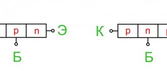
Transistors consist of the following circuit. This is primarily a nest of charge carriers or, in other words, a source. It is a kind of emitter of a bipolar transistor.
Next comes the socket for receiving charge carriers or drain. It is similar to the collector type of bipolar equipment.
Another important part of the transistor is called the gate. It controls the electrodes and is somewhat reminiscent of the base of a bipolar device.
It is impossible not to note the shutter, of which there may be several in the device. Without them, there is no way to build a chain of microcircuits or secure programmable memory cells.
In this case, semiconductor devices can operate in the following state:
- with generating oscillation;
- with negative potential;
- closed (the device will produce the maximum direct voltage).
MOS transistor (MOSFET) device with an induced channel.
On the base (substrate) of a semiconductor with P-type electrical conductivity (for a transistor with an N-channel), two zones with increased N+-type electrical conductivity are created. All this is covered with a thin layer of dielectric, usually silicon dioxide SiO2. Metal leads from N+-type regions, called drain and source, pass through the dielectric layer. Above the dielectric is a metal gate layer. Sometimes a lead also comes from the substrate, which is short-circuited with the source
Shutter charge
Although the input capacitance value is a fairly useful value, even knowing it, it is quite difficult to compare the key characteristics of two MOSFETs from different manufacturers. The effects associated with different device sizes, as well as the steepness of the characteristic, make such a comparison quite difficult. More accurate results can be obtained by considering not the input capacitance, but the total charge that must be supplied/extracted from the gate to change the state of the transistor. Most manufacturers indicate both capacity and full charge in the instructions. Rice. 13 shows a circuit for measuring the total gate charge.
Rice. 13. a) Circuit for measuring the total charge of the gate; b) and mutual processes at the gate and drain when the transistor opens
The advantage of using the full gate charge as a characteristic of the transistor is that the designer can quite easily calculate the approximate gate current required to switch the transistor in a certain time using the formula I
=
Q
/Δ
t
. For example, a device with a gate charge of 20 nC can be turned on/off in 20 μs with a gate current of 1 mA or in 20 ns with a gate current of 1 A.
Operation of a MOS transistor (MOSFET) with an N-type induced channel.
Let's connect a voltage of any polarity between the drain and source. In this case, no electric current will flow, since between the N+ zones there is a region P that does not allow electrons to pass through. Further, if a positive voltage is applied to the gate relative to the source Uzi, an electric field will arise. It will push positive ions (holes) from the P zone towards the substrate. As a result, the concentration of holes under the gate will begin to decrease, and their place will be taken by electrons attracted by the positive voltage on the gate.
When Uzi reaches its threshold value, the electron concentration in the gate region will exceed the hole concentration. A thin channel with N-type electrical conductivity will be formed between the drain and the source, through which the current Ic will flow. The higher the voltage at the gate of the transistor Uzi, the wider the channel and, therefore, the greater the current. This mode of operation of a field-effect transistor is called enrichment mode.
The operating principle of an MOS transistor with a P-type channel is the same, only a negative voltage must be applied to the gate relative to the source.
Dynamic characteristics
When using a MOSFET transistor as a power switch, its main function is to turn on/off the drain current based on a signal at the gate. Rice. 11a illustrates the Ic
(
Uzi
), and fig. 11(b) is an equivalent circuit often used in analyzing key properties of MOSFETs.
Rice. 11. a) Slopeness as a characteristic of a transistor; b) equivalent circuit indicating the elements that most strongly influence switching
Key properties are determined by the time required to establish certain voltages on stray capacitances. Distributed gate resistance Rg
approximately inversely proportional to the cell area.
The inductances of the source Ls and drain Ld terminals are on the order of tens of nH. Typical values of input ( Ciss
) and output (
Coss
) capacitances, as well as feedback capacitance
Crss
, are given in the transistor descriptions and are used by developers to determine the ratings of the components included in the circuit. These capacitances are defined in terms of equivalent circuit capacitances as follows:
Gate-drain capacitance CGD
is a nonlinear function of voltage and is the most important parameter, since it forms a feedback loop between the input and output of the transistor.
It is also called Miller capacitance because it has the effect of increasing the input capacitance in dynamic mode, when it is no longer equal to the simple sum of the capacitances. In Fig. Figure 12 shows a typical scheme for measuring switching time, and also shows the rise and fall intervals of USI
and
USI
.
Rice. 12. a) Switching speed measurement circuit; b) mutual behavior of gate-source and drain-source voltages
Current-voltage characteristics (CV characteristics) of a MOS transistor with an induced channel.
The current-voltage characteristics of a field-effect transistor with an insulated gate are similar to the current-voltage characteristics of a field-effect transistor with a control PN junction. As can be seen in graph a), initially the current Ic increases in direct proportion to the increase in voltage Uc. This area is called the ohmic region (Ohm's law applies), or the saturation region (the transistor channel is saturated with charge carriers). Then, when the channel expands almost to its maximum, the current Ic practically does not increase. This area is called the active region.
When Uc exceeds a certain threshold value (the breakdown voltage of the PN junction), the structure of the semiconductor is destroyed and the transistor turns into an ordinary conductor. This process cannot be restored, and the device becomes unusable.
Steepness
gfs slope
is a measure of the sensitivity of the drain current to changes in the control voltage
UZ
.
This parameter is usually determined in the range of voltage values USI
, which gives half the maximum drain current, and for the range of values of
USI
, in which the drain current is constant across
USI
(saturation region). The transconductance is affected by the gate width, which increases relative to the active region of the cell with increasing cell density. This density has historically increased from an approximate figure of 80 thousand cells per square centimeter in 1980 to values of 1.2 million (for planar transistors) and 1.9 million (for trench transistors) at present. The limiting factor for further growth is the difficulty of controlling the photolithographic process and the difficulty of creating reliable contact with the metallization of the source in the center of the cell.
The slope value is also influenced by the channel length and the thickness of the gate oxide layer. To increase the steepness and reduce the resistance of the switched-on transistor, it is necessary to reduce the length of the channel, but this tendency is restrained by the phenomenon of through puncture described above.
Operation of an MOS transistor (MOSFET) with a built-in N-type channel.
Let's connect the voltage between the drain and source Ui of any polarity to the transistor. Let's leave the shutter disabled (Uzi = 0). As a result, a current Ici, which is a flow of electrons, will flow through the channel.
Next, we connect a negative voltage to the gate relative to the source. A transverse electric field will arise in the channel, which will begin to push electrons out of the channel zone towards the substrate. The number of electrons in the channel will decrease, its resistance will increase, and the current Ic will decrease. As the negative gate voltage increases, the current decreases. This state of operation of the transistor is called depletion mode.
If a positive voltage is applied to the gate, the resulting electric field will attract electrons from the drain, source, and substrate regions. The channel will expand, its conductivity will increase, and the current Ic will increase. The transistor will enter enrichment mode.
As we can see, a MOS transistor with a built-in channel is capable of operating in two modes - in depletion mode and in enrichment mode.
Voltage drop across internal diode
Internal pn
- the transition is closed during normal operation of the transistor (with normal drain-source voltage polarity).
This junction opens when the polarity of the applied voltage is reversed. Being a parasitic element, it can, at the same time, be used circuit-wise as a protective device. The forward drop across the open internal diode is determined by the VF
.
VF
indicates the guaranteed maximum value of this characteristic at a certain value of the source current.
In Fig. Figure 10 shows typical I-V characteristics of an internal diode at two temperatures. Due to the higher contact resistance between metallization and p
-type
channel
devices have a higher voltage
VF
than
n
-type devices.
Normal VF
are 1.6 V for high voltage (>100 V) and 1.0 V for low voltage (<100 V).
Rice. 10. Current-voltage characteristic of an open internal diode
Advantages and disadvantages of field-effect transistors over bipolar ones.
Field-effect transistors have practically replaced bipolar transistors in a number of applications. They are most widely used in integrated circuits as keys (electronic switches)
The main advantages of field-effect transistors
- Due to the very high input resistance, the field-effect transistor circuit consumes extremely little energy, since it consumes virtually no input current.
- The current gain of field-effect transistors is much higher than that of bipolar transistors.
- The noise immunity and reliability of operation are significantly higher, since due to the absence of current through the gate of the transistor, the control circuit on the gate side is isolated from the output circuit on the drain and source sides.
- Field-effect transistors have an order of magnitude higher speed of transition between the states of conduction and non-conduction of current. Therefore, they can operate at higher frequencies than bipolar ones.
The main disadvantages of field-effect transistors
- FETs have a higher voltage drop due to the high resistance between drain and source when the device is in the on state.
- The structure of field-effect transistors begins to deteriorate at a lower temperature (150C) than the structure of bipolar transistors (200C).
- Despite the fact that field-effect transistors consume much less energy compared to bipolar transistors, when operating at high frequencies the situation changes dramatically. At frequencies higher than approximately 1.5 GHz, the power consumption of MOSFETs begins to increase exponentially. Therefore, the speed of processors stopped growing so rapidly, and their manufacturers switched to a “multi-core” strategy.
- When manufacturing high-power MOS transistors, a “parasitic” bipolar transistor appears in their structure. In order to neutralize its influence, the substrate is short-circuited with the source. This is equivalent to shorting the base and emitter of the parasitic transistor. As a result, the voltage between the base and emitter of the bipolar transistor will never reach the voltage required for it to open (about 0.6V is required for the PN junction inside the device to begin conducting).
However, if there is a rapid voltage jump between the drain and source of the field-effect transistor, the parasitic transistor may accidentally open, as a result of which the entire circuit may fail.
- The most important disadvantage of field-effect transistors is their sensitivity to static electricity. Since the insulating dielectric layer on the gate is extremely thin, sometimes even a relatively low voltage is enough to destroy it. And discharges of static electricity, present in almost every environment, can reach several thousand volts.
Therefore, they try to create the external housings of field-effect transistors in such a way as to minimize the possibility of unwanted voltage occurring between the electrodes of the device. One such method is to short-circuit the source with the substrate and ground them. Also, some models use a specially built-in diode between the drain and source. When working with integrated circuits (chips) consisting primarily of field-effect transistors, it is advisable to use grounded antistatic wrist straps. When transporting integrated circuits, vacuum antistatic packaging is used
What is it needed for
PTs are needed to control the output current using the generated electric field and change its most important parameters. Structures based on field-effect transistors are often used in digital and analog integrated circuits.
n- and p-channel electrotransistors
It is through field control that these transistors influence the magnitude of the voltage applied to their gate. This distinguishes them from bipolar transistors, which are controlled by the current that flows through their base. PTs consume significantly less electricity, which determines their popularity when used in waiting and tracking devices, as well as low-consumption integrated circuits (when organizing sleep mode).
You might be interested in this. Features of SHDUP U4
Important! Some of the most famous devices based on the action of field-effect transistors are TV remote controls and electronic wristwatches. Due to their design and the use of DC, these devices can operate for years from one tiny power source in the form of a battery.
Schematic view of a field-effect transistor
Application of a blocking layer in JFET transistors
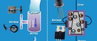
But where can the property “change in dielectric thickness under the influence of electric field strength” be applied? Let's look at a small example. Maybe later it will become clear to you where this property can be applied 
So, provincial town X. An ordinary weekday. A stream of people is rushing about their business. There is a hot dog stand near the sidewalk. It hasn’t opened yet, as the seller is sleeping soundly, so everyone passes by this shop:
But then it opens, and the first onlookers begin to “hang out” near it to taste the cold, rotten hot dogs from the day before yesterday)).
The seller sees that business is improving and begins to serve customers even faster. That is, he puts all his energy into maintaining the pace. He starts working harder . The more intensely he serves clients, the more of them there are. Onlookers are interested in what kind of party is planned there. And since everyone is buying, then they want it too. There are a little more people.
People are quietly pouring in and the seller, in order not to miss the profit, begins to work with all his might. Our poor salesman works like a squirrel in a wheel. You can’t relax here anymore, otherwise people will go to the donut seller. There was sweat on his forehead, tense that he was about to burst from fatigue! But look at the sidewalk... The traffic was blocked by onlookers who wanted to buy these rotten hot dogs.
The moral of this story is:
If you want to eat, cook it in the morning).
Now let's imagine that the sidewalk is a conductor. People are electrons. The seller is some kind of charge who, if he wants, can either work harder or close the shop altogether.
So what do we have then? While the shop is closed, a crowd of onlookers calmly goes about their business in one direction. The seller is not there. That is, the charge is zero. This means that electric current flows calmly in this direction, since the ordered movement of charged particles is electric current
As soon as the seller opened the shop and began to work, some onlookers began to crowd around the shop. But this bunch of onlookers are now getting in the way on the sidewalk for people who are really in a hurry somewhere on business. That is, this bunch of yawns resists the flow of people rushing about business. Already more interesting. If they get in the way, it means fewer people will be able to pass below the crowd of onlookers in any given time. What does this parameter mean to us? Isn't the current strength by chance? That's it! The current strength has become less!
So, now the main question is: what determines the flow of people? Yes, from the seller, his mother's leg!
As soon as he starts yelling: “Get some fresh hot dogs, come and buy them for your mother-in-law!”, more people appear. That is, as soon as he starts working harder , the crowd of onlookers begins more . And it could all end with traffic on the sidewalk becoming a standstill. And yes, by the way. A standing crowd of onlookers are no longer electrons. This is the depletion layer, dielectric)
And so, scientific engineers who realized that it was possible to change the strength of the current by controlling the strength of the electric field, created a radio element, which they named after the electric field, and its name is field-effect transistor .