In everyday life, a powerful power source with a fixed voltage is often needed. It can be used as a charger, to power audio equipment (amplifiers), etc. It is advisable to make such power supplies using a pulse circuit. This circuitry allows you to create lightweight and powerful DC voltage sources. The complexity of the circuit begins to fade into the background compared to its advantages already at load currents of more than 2A. You can make a switching power supply with your own hands if you have the equipment and certain qualifications.
Types and principle of operation of switching power supplies
The basic operating principle of a switching power supply (SMPS) is that direct voltage (rectified mains voltage or from a third-party source) is converted into pulsed voltage with a frequency of up to hundreds of kilohertz. Due to this, the winding parts (transformers, chokes) are light and compact.
Fundamentally, IIPs are divided into two categories:
- with pulse transformer;
- with storage inductance (it can also have secondary windings)
The former are similar to conventional transformer mains power supplies; their output voltage is regulated by changing the average current through the transformer winding. The latter work on a different principle - they are regulated by changing the amount of accumulated energy.
Based on other characteristics, IIP can be divided into unstabilized and stabilized, unipolar and bipolar, etc. These features are not of such a fundamental nature.
Peak power
Despite these disadvantages, when powering the amplifier from an unstabilized source, you can get some bonus - short-term (peak) power is higher than the power of the power supply due to the large capacity of the filter capacitors. Experience shows that a minimum of 2000uF is required for every 10W of output power. Due to this effect, you can save on the power transformer - you can use a less powerful and, accordingly, cheaper transformer. Keep in mind that measurements on a stationary signal will not reveal this effect; it appears only during short-term peaks, that is, when listening to music.
A stabilized power supply does not have this effect.
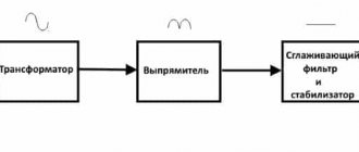
Structural and schematic diagram of the main parts of the block
Generalized block diagram of a pulse power supply.
A surge filter is installed at the input of the power supply. In principle, it does not affect the operation of a homemade or industrial switching power supply - everything will function without it. But you cannot abandon the filtering circuit - due to the extremely nonlinear shape of the consumed current, pulsed sources intensively “sprinkle” interference into a 220-volt household network. For this reason, devices running on the same network on microprocessors and microcontrollers - from electronic watches to computers - will malfunction.
Network filter circuit.
The purpose of the input device is to protect against two types of interference:
- common-mode (asymmetrical) – occurs between any wire and the ground (case) of the power supply unit;
- differential (symmetrical) – between the power wires (poles).
The filter, like the entire power supply, is protected at the input by fuse F (fuseable or self-recovering). After the fuse there is a varistor - a resistor whose resistance depends on the applied voltage. As long as the input voltage is normal, the resistance of the varistor is high and it has no effect on the operation of the circuit. If the voltage increases, the resistance of the varistor drops sharply, which causes an increase in current and the fuse burns.
Capacitors Cx block differential noise at the input and output of the filter in the range up to 30 MHz. At a frequency of 50 Hz their resistance is high, so they do not affect the mains voltage. Their capacitance can be selected from 10 to 330 nF. Resistor Rd is installed for safety - the capacitors are discharged through it after the power is turned off.
Common-mode interference is suppressed by a filter on Cy and L. Their values for the cutoff frequency f are related by the Thompson formula:
f=1/(2*π*√L*C) , where:
- f – cutoff frequency in kHz (the conversion frequency of the pulse generator is taken);
- L – inductance of the inductor, μH;
- C – capacitance Cy, µF.
The common mode choke is wound on a ferrite ring. The windings are identical, winding on opposite sides.
Common mode choke design.
Unlike the output filter, the rated current of the power supply unit does not affect the calculation of the noise protection filter elements, with the exception of the wire with which the inductor is wound.
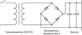
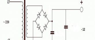
After the filter, the mains voltage is rectified. In most cases, a standard full-wave bridge rectifier is used.
Identifying Sources of Common Mode Interference
Accounting for the differential component
In the absence of a special differential noise filter in the power supply, its share in the common-mode component supplied to the network can be quite significant (see example above). The source of interference can be considered voltage Udiff - the voltage at the input of the power source (after the filter). Here L1, C1, C2 constitute a standard common mode filter circuit. In this case, the differential component passes through the common-mode filter choke without interference and is separated with the corresponding sign on the voltage divider formed by the test resistors (Fig. 3). Coupling capacitors are not shown, since their impedance in the frequency band under consideration can be neglected. The voltage Udiff can be determined quite well based on the analysis of electrical processes in the converter; in particular, the high-frequency ripple on the input capacitor included in the power source can be taken as Udiff. As can be seen, the differential component is not at all suppressed by the common-mode filter and can be present in the measured signal as a result of applying the measurement technique from [1]. A good method for eliminating this component from the interference signal is to use an additional differential noise filter (in the simplest case, an LC filter).
Rice. 3. Differential component of interference
Taking into account the common mode component
However, the main component of noise relative to ground (especially with a good differential noise filter) is precisely common-mode noise - that is, noise that is the same for both input terminals of the power supply in a given frequency range. For this case, the equivalent circuit shown in Fig. 4.
Rice. 4. Common mode component of interference
The interference signal Usinf is allocated to the Y-capacitors of the filter (for a given equivalent circuit they are connected in parallel), as a result of dividing the voltage of some effective interference source Uef by a capacitive divider with a transfer coefficient (1), the upper arm of which forms the effective capacitance Cef.
The greater the total capacitance of the Y-capacitors Cy compared to Cef, the lower the interference voltage. Note that restrictions on increasing the capacity of Y-capacitors are imposed by safety standards that normalize the maximum permissible leakage current. Next, the interference signal is filtered by an LR filter with a transmission coefficient (2), composed of the inductance of the common-mode choke L1 and test resistances R, connected in parallel, according to the equivalent circuit (Fig. 4).
The task of determining Ueff and Cef in the general case is nontrivial. Its solution will depend on the applied power supply circuit, components, design and technology. In the simplest case, Cef is determined by the interwinding capacitance of the power transformer, and Ueff is determined by the voltage applied between its windings. Obviously, the greater the inductance of inductor L1, the more suppressed common-mode interference is.
Inverter circuits
The resulting rectified voltage is supplied to the converter (inverter). It is performed on bipolar or field-effect transistors, as well as on IGBT elements that combine the properties of field-effect and bipolar ones. In recent years, high-power, low-cost insulated gate field-effect transistors (MOSFETs) have become widespread. It is convenient to build key inverter circuits on such elements. Switching power supply circuits use various options for connecting MOSFETs, but push-pull circuits are mainly used due to their simplicity and the ability to increase power without significant modifications.
Push-pull scheme
Push-pull converter circuit.
A push-pull inverter (push - push, pull - pull) is an example of a push-pull converter. Transistor switches operate on the primary winding of the transformer, consisting of two half-windings I and II. The transistors open alternately for a given period of time. When the top transistor in the circuit is open, current flows through half-winding I (red arrow), when the second one flows through half-winding II (green). To avoid a situation where both switches are open (due to the finite speed of the transistors), the control circuit creates a pause called Dead time.
Transistor control taking into account Dead time.
This circuit works well at low supply voltage (up to +12 volts). The downside is the presence of surges with an amplitude equal to twice the supply voltage. This entails the use of transistors designed for twice the voltage.
Bridge circuit
The push-pull bridge is free from the main drawback of the previous scheme.
Push-pull bridge inverter circuit.
Here, a pair of transistors T1 and T4 , then T2 and T3 (the key control signal is generated taking into account Dead time). In this case, the primary winding is connected to the power source first on one side, then on the other. The pulse amplitude is equal to the full supply voltage, and there are no voltage surges. The disadvantages include the use of four transistors instead of two. In addition to increasing the size of the power supply, this leads to doubled voltage losses.
Half bridge circuit
In practice, a half-bridge inverter circuit is often used - to a certain extent, a compromise between the previous two circuits.
Half-bridge circuit.
In this case, one side of the winding is switched by alternately opening transistors T1 and T2, and the other is connected to the midpoint of the capacitive divider C1, C2. Advantages of the scheme:
- unlike push-pull, there are no voltage surges;
- unlike bridge, only two transistors are used.
On the other side of the scale, the transformer winding is powered by only half the supply voltage.
Single-ended circuits
In the circuitry of converters, single-cycle circuits are also used - forward and flyback. Their fundamental difference from push-pull ones is that the transformer (more precisely, its primary winding) simultaneously serves as a storage inductance. In flyback circuits, energy is accumulated in the primary winding during the open state of the transistor, and is transferred to the load through the secondary winding during the closed state. In direct thrusters, energy accumulation and release to the consumer occur simultaneously.
Two phases of operation of a flyback single-cycle inverter.
Pulse IP controller
The controller is the basis of the inverter, so we will describe it in more detail. The inverter uses a TL494 controller with a set operating frequency the same as in ATX power supplies, that is, 30 kHz. The inverter does not have output voltage stabilization, so the controller operates with a maximum duty cycle of 85%. The controller is equipped with a soft start system consisting of elements C5 and R7. After starting the inverter, the circuit provides a smooth increase in the duty cycle starting from 0%, which eliminates the charging surge of the output capacitors. The TL494 can operate from 7 V, and this voltage supplying the buffer of the control transformer T2 causes the generation of a voltage at the gates of the order of 3 V. Such not fully open transistors will output tens of volts, which will lead to huge power losses and there is a high probability of exceeding the dangerous limit. To prevent this, protection is provided against too high a voltage drop. It consists of a resistor divider R4 - R5 and transistor Q1. After the voltage drops to 14.1 V, Q1 discharges the soft start capacitor, thereby reducing the charge to 0%.
Another function of the controller is to protect the inverter from short circuit. Information about the primary winding current is obtained by the controller through the current transformer T3. The current in the secondary winding T3 flows through resistor R9, across which a small voltage drops. Information about the voltage on R9 is sent via potentiometer PR1 to the error amplifier TL494 and compared with the voltage of the resistor divider R1 and R2. If the controller detects a voltage higher than 1.6 V on potentiometer PR1, it turns off the transistors before they cross the dangerous limit and is latched through D1 and R3. The power transistors remain off until the inverter is restarted. Unfortunately, this protection only works correctly on the +/- 35 V line. The +/- 12 V line is much weaker and in the event of a short circuit there may not be enough current for the protection to operate.
The controller's power supply is transformerless using capacitor resistance. The two capacitors C20 and C24 consume reactive energy from the mains and hence by causing current to flow, they charge the filter capacitor C1 through the rectifier D10-D13. Zener diode DZ1 protects against too high voltage on C1 and stabilizes them at 18 V.
Power transformer
The power transformer operates at high frequencies (up to several tens of kilohertz), so it can be made on a core made of ferrite rather than transformer iron. Also, due to the increased frequency, its dimensions will be smaller than that of a network one, designed for conversion at a frequency of 50 Hz. The calculation of a pulse transformer is quite extensive. You can understand it for general development, but for practical purposes it is better to use some program, including online services.
Interface of the Lite-CalcIT program.
The Lite-CalcIT program is popular. She can calculate a transformer for an existing core, or she can select the optimal one based on the entered data.
Snubber
To compensate for current and voltage surges that inevitably arise when switching the primary winding of a transformer, damper circuits are used, called snubbers in English technical literature. Such circuits can be installed along the power supply (parallel to the primary winding of the transformer) or separately on each switch. The design of snubbers can be different, but the most widespread are dampers in the form of a sequential RC chain (diagram b in the figure).
Various damper schemes.
There is no substantiated method for calculating a snubber. To do this, it is necessary to take into account all parasitic inductances (windings, tracks, capacitors) at many frequencies and for unknown wave impedances. Therefore, all existing calculations are empirical in nature.
The main (and only) active element of the damper is the capacitor. It “absorbs” impulse emissions. The resistor only worsens the damping properties, but limits the current through the capacitor, which can reach significant values, albeit for a short time. This scheme is more relevant in thyristor converters.
You can find out what a snubber or damper is by watching the video.
The RCD snubber circuits (c and d in the figure) contain diodes. They can be useful for limiting reverse polarity pulses in thyristor and bipolar transistor circuits. If the switches are assembled on field-effect or IGBT transistors, then there is no point in installing valves - they duplicate the diodes present inside these transistors.
The capacitance of the capacitor is selected in the range of 0.1–0.33 μF. In 90+ percent of cases this is enough. An increase or decrease in value is used for keys operating under non-standard conditions (increased conversion frequency, etc.)
Rectifier
The voltage of the secondary winding must be rectified. For levels up to 12 volts, it is advisable to use a full-wave, midpoint circuit.
Diagram of a rectifier with a midpoint and the passage of current through it.
The advantage of this circuit is that the current flows in each direction through only one diode, and the voltage drop across the valves, in contrast to the classic bridge circuit, is half as much. This can significantly reduce the required number of turns of the secondary winding. The same purpose is served by the use of Schottky diodes and assemblies of them.
Bridge rectifier circuit and current flow through it.
If the output voltage of the power supply is higher than +12 volts, then saving 0.6 volts becomes insignificant, and you can make a rectifier according to the standard circuit and use a transformer without a tap.
If the output of a switching power supply must be bipolar, tapping from the midpoint again becomes rational. In this case, 4 diodes and radiators for them are saved at once - the gain in size can be significant.
Bipolar rectifier with midpoint.
Calculation examples
Calculation at one point
As a first example, let us consider the calculation of the level of common mode interference for a converter, the experimental characteristics of which were shown in Fig. 2. In this case, the task of analysis is rather set - to test the methodology and compare it with experimental results.
In this case, the common-mode component of the interference signal Usinf was first calculated (Fig. 4), which for this mode was rectangular voltage pulses with a peak-to-peak swing (from peak to peak) dU1 (3), where Vin, Vo are the input and output voltages of the converter, w1, w2 is the number of turns in the primary and secondary windings of the power transformer. The converter is a flyback converter, operating at a given Vin in continuous current mode and duty cycle G = ti/T.
Then the signal Usinf was decomposed into harmonics using the fast Fourier transform procedure and multiplied by the filter transmission coefficient Ks (2). The resulting signal was then reconstructed in the time domain using an inverse fast Fourier transform. In this way, the common-mode component in the measured signal was obtained.
After this, a differential component was added to the received signal with the appropriate sign (Fig. 3), defined as the product of the current in the input capacitor of the converter and its ESR (equivalent series resistance). The differential component in this case was determined by (4), where I0 is the initial value of the current of the primary switch of the converter, L is the magnetizing inductance. Note that the initial value of the current I0 in this case was close to zero, that is, the block was close to the boundary mode. It should also be noted: the addition of signals on test resistors was carried out without taking into account their constant components, which made it possible to significantly simplify calculations in the time domain. As a result, idealized diagrams of voltages on the measuring resistors were obtained (Fig. 5), which can be compared with experimental oscillograms (Fig. 2): at 0 < t < GT,
Where
for GT< t< T Udiff = 0.
Rice. 5. Idealized voltage diagrams on measuring resistors
The spectral composition (up to the 7th harmonic) of these time characteristics is presented in Fig. 6. Despite some differences from the characteristics calculated from experimental data, it can be argued that, to a first approximation, the calculation gives correct results.
Rice. 6. Spectral composition of voltages on measuring resistors
In conclusion, we present the values of all parameters used in the calculations of this example:
- Vin = 60 V — converter input voltage;
- Vo = 24 V - output voltage of the converter;
- Io = 1.25 A - output current of the converter;
- w1 = 60, w2 = 27 - turns of the power transformer;
- T = 10 μs - switching period;
- G = 0.48 - duty cycle (duty factor);
- Cef = 62 pF - interwinding capacitance of the power transformer;
- Cy = 4.4 nF - total capacity of Y-capacitors;
- Ls = 3.8 mH - inductance of the common-mode choke;
- L = 40 nH - magnetizing inductance of a power transformer reduced to a unit turn;
- ESR = 20 mOhm - equivalent series resistance of the input capacitor;
- I0 = 0.06 A - current value of the primary switch of the converter at t = 0;
- R = 50 Ohm - test resistor value.
Calculation with variation of parameters
Calculation at one point does not always satisfy the designer, since the converter parameters (for example, input voltage) may change. Based on knowledge of the nature of the influence of certain parameters, the developer can make the final choice of common-mode interference filter parameters.
As an example, let us consider how the harmonic composition of the differential and common-mode components of the noise measured at the test resistor will change depending on the supply voltage of the power source. This example concerns a series of power supplies designed for an extended input voltage range (85–342 Vdc) and an output power of 30 W. For this series of power supplies, a calculation was made of the dependence of the amplitudes of the first five harmonics, measured on the test resistor (Fig. 1), on the input voltage of the converter. In Fig. Figure 7 shows the results of this calculation for the worst case in a series of output voltages (Vo = 5 V).
Rice. 7. Differential (left) and common-mode (right) interference components for the first five harmonics
It can be seen from the figure that in terms of the differential component the unit cannot satisfy the requirements of GOST [1] and it is necessary to introduce a differential noise filter. In terms of common mode interference, when using a common mode choke rated 8.2 mH, the units fall into Class A (industrial use). The exit from the Class B group occurs at the second harmonic at Vin > 200 V. Increasing the inductance of the common mode choke by 20% will allow, according to the calculation, to satisfy the requirements of Class B (domestic use).
Filter
The output voltage must be filtered - it contains a large number of conversion products. Since the inverter operates at a fairly high frequency, filters containing not only capacitors, but also small-sized chokes with relatively low inductance become effective.
L- and U-shaped LC filters.
To calculate the filter elements, it is necessary to specify the pulsation coefficient Kp. It is selected from the expected load:
- sensitive equipment for radio reception, preliminary stages of audio equipment, microphone amplifiers - Kp = 10-5..10-4 ;
- audio frequency amplifiers – Кп=10-4..10-3 ;
- middle and low class receiving and sound reproducing equipment – Kp=10-2..10-3 .
For an L-shaped filter installed after a full-wave rectifier, the following relations apply:
- L*C=25000/(f2+Kp);
- L/C=1000/R2н.
In these formulas:
- L – inductance of the inductor in µH;
- C is the capacitance of the capacitor in microfarads;
- f – conversion frequency in Hz;
- Rн – load resistance in Ohms.
For U-shaped filter:
- С1=С2=С;
- L/C=1176/R2н.
The dimension of the values is the same as for the previous filter.
Circuits and manufacturing of switching power supplies
Switching power supplies are assembled on various element bases. Typically, specialized microcircuits specially designed for creating such devices are used to build SMPS. Except for the simplest blocks.
Powerful pulse unit on ir2153
Simple power supplies can be built on the IR2153 chip. It is a powerful integrated driver with a timer similar to the NE555. The generation frequency is set by external elements. The microcircuit does not have inputs for organizing feedback, so current and voltage stabilization cannot be obtained using the PWM method.
Pin layout of the IR2153 chip.
The assignment of the pins is given in the table.
| № | Designation | Purpose | Purpose | Designation | № |
| 1 | Vcc | Power supply for logic and drivers | Power output switches | Vb | 8 |
| 2 | Rt | Frequency setting resistor | Top Driver Output | HO | 7 |
| 3 | Ct | Frequency setting capacitor | Top Driver Power Return | Vs | 6 |
| 4 | COM | General | Bottom Driver Output | L.O. | 5 |
Internal circuit of IR2153.
To better understand the operation and pin assignments, it is best to study the internal circuitry. The main point that you need to pay attention to is that the output switches are assembled using a half-bridge circuit.
Using this chip you can assemble a simple power supply.
Scheme of a simple power supply based on IR2153.
The IR2153 is powered by 220 volts through a quenching resistor R1, a diode rectifier VD3, and a filter on C4. The generation frequency is set by elements C5, R2 (with the values indicated in the diagram, it turns out to be about 47 kHz). A transformer can be considered a program. The author's version used a power transformer from a computer power supply. The standard windings have been removed, the primary is wound into two cores with enamel insulated wire with a diameter of 0.6 mm.
Add a link to a discussion of the article on the forum
RadioKot >Schemes >Power supply >Power supplies >
| Article tags: | Add a tag |
200 W switching power supply for UMZCH
Author: Alexey Malyshev Published 09/06/2012 Created with the help of KotoEd. Participant of the Competition “Congratulate the Cat as a Human Being 2012!”
Hello dear Cat! Happy birthday to you and all the best, so to speak! And as a gift, accept such a very useful thing as a power supply for an amplifier.
ATTENTION!
Some elements of this device are exposed to life-threatening mains voltage! Some elements retain a dangerous electrical charge after the device is unplugged! Therefore, when installing, setting up and working with the device, it is necessary to comply with electrical safety requirements. By repeating the device, you act at your own peril and risk. I, the author, do NOT bear any responsibility for any moral and material damage, damage to property, health and life caused as a result of repetition, use or inability to use this design.
So, let's begin.
Disputes about whether a switching power supply is good or bad for UMZCH (hereinafter referred to as SMPS) are beyond the scope of this article. Personally, I believe that a properly designed, soldered and adjusted SMPS is no worse (and in some respects even better) than a classic power supply with a network transformer.
In my case, the use of SMPS was necessary because I wanted to fit my amplifier into a flat case.
Before developing this SMPS, I studied many ready-made circuits available on the Internet and in the literature. Thus, among radio amateurs, different versions of the unstabilized SMPS circuit on the IR2153 chip are very popular. The advantage of these schemes is only one – simplicity. As for reliability, it is nonexistent - the IC itself does not have overload protection and soft start functions for charging output electrolytes, and the addition of these functions deprives the SMPS of its advantage - simplicity. In addition, the implementation of a soft start on this IC is extremely doubtful - it does not allow changing the pulse width, and methods based on changing the operating frequency of the IC are ineffective in a “regular” half-bridge SMPS and are applicable in resonant converters. I somehow didn’t really want to blast electrolytes and keys with huge currents when turning on the unit.
The possibility of using the well-known TL494 IC was also considered. However, upon deeper study, it turned out that for reliable operation around this IC you will have to hang a bunch of all sorts of transistors, resistors, capacitors and diodes. And this is no longer “our method” 
As a result, the choice fell on a more modern and faster chip called UC3825 (Russian analogue of K1156EU2). A detailed description of this IC can be found in its Russian datasheet [1] and in the Radio magazine [2].
For those who are too lazy to read these sources, I will say that this is a high-speed PWM controller with the following capabilities:
- Control of powerful MOS transistors.
- Work in devices with voltage and current feedback.
- Operation at frequencies up to 1 MHz.
- The delay of the signal passing through the circuit is 50ns.
- Half-bridge outputs for current up to 1.5A.
- Wideband error amplifier.
- Presence of PWM latch.
- Current limitation in each period.
- Smooth launch. Limitation of the maximum output pulse duration.
- Undervoltage protection with hysteresis.
- Switching off the circuit by an external signal.
- Accurate voltage reference (5.1V +/- 1%).
- Housing “DIP-16”
Well, exactly what you need! Let us now consider the SMPS itself.
Specifications
Input voltage, V…………………………………………….. 176…265;
Rated total load power, W………………. 217.5;
The level of the control signal at which the power supply is turned on………Log. 1 CMOS;
Signal level at which the power supply is turned off…………………… <0.6 V or NC;
Efficiency at maximum load, %……………………………80;
Dimensions (LxWxH), mm………………………………………………………..212x97x45
Output voltages
| Output voltage, V | Minimum load current, A | Maximum load current, A |
| ± 25 | 0,24 | 4 |
| ± 15 | 0 | 0,5 |
| + 5 (on duty) | 0 | 0,5 |
Schematic diagram
The schematic diagram of the SMPS is shown in the figure.
The architecture of this power supply is reminiscent of the SMPS of ATX format computers. The mains voltage is supplied through fuses FU1 and FU2 to the surge protector and standby power transformer. The use of two fuses is necessary for safety reasons - with one common fuse, in the event of a short circuit in the T1 winding, the current in its circuit will be insufficient to blow this fuse, and the power released by the failed transformer is sufficient to ignite it.
The surge filter contains a two-winding inductor L1, X-capacitors C1, C2 and Y-capacitors C3, C4 and has no special features. Varistor RV1 protects the SMPS from high-voltage surges in the network and when the network voltage exceeds the maximum permissible value.
NTC thermistor RK1 limits the charging current of capacitor C5 when the SMPS is connected to the network.
The voltage rectified by bridge VD1 and smoothed by capacitor C5 is supplied to a half-bridge inverter formed by MOS transistors VT1, VT2 and capacitor divider capacitors C6, C7. The separate construction of the input filter and capacitive divider makes it possible to facilitate the operation of the oxide filter capacitor, which has a relatively large ESR value. Resistors R5, R6 equalize the voltage on the divider capacitors.
The T4 power pulse transformer is included in the diagonal of the half-bridge.
The output circuits of the SMPS contain rectifiers using diodes VD5 - VD8, VD9 - VD12, a group stabilization choke (GS) L3 and U-shaped filters C11 - C16, L4, L5 and C17 - C22, L6, L7. Ceramic capacitors C13, C14, C17, C18 facilitate the operation of the corresponding electrolytes. Resistors R11 – R14 create the initial load necessary for normal operation of the SMPS at idle.
Chains C8, R7; C9, R9; C10, R10 – damping. They limit emissions of EMF, self-inductance, and leakage inductance and reduce the interference created by SMPS.
The control circuit did not fit on the main board, so it was assembled in the form of an A1 module on an additional board.
As you probably already guessed, its basis is the DA2 UC3825AN chip. It is powered by an integral stabilizer on the KRENK DA1. Capacitors C1 and C7 – power filter. They, as the DS says, should be located as close as possible to the corresponding DA2 pins. Capacitor C5 and resistor R8 are frequency-setting. With the ratings indicated in the diagram, the conversion frequency of the power supply is approximately equal to 56 kHz (the operating frequency of the IC is 2 times higher - after all, we have a push-pull SMPS). Capacitor C4 sets the duration of the soft start, in this case 78 ms. Capacitor C2 filters noise at the output of the reference voltage source. Elements C6, R9, R10 are the error amplifier compensation circuit, and R4, R6 are the output voltage divider of the power supply unit, from which the feedback signal is removed.
Overcurrent protection is implemented on current transformer T3. The signal from its secondary winding is rectified by a rectifier using diodes VD3, VD4 (main board). Resistor R8 (on the main board) is the current transformer load. The signal from R8 through the filter chain R7, C3 (in module A1) is supplied to the current limiting input DA2. This power supply unit implements clock-by-clock current limitation, i.e. the microcircuit does not allow the current through the switches to build up to dangerous values. When the voltage reaches 1 V at pin 9, the microcircuit limits the pulse width. If a short circuit occurs in the load and the switch current increases faster than DA2 has time to react to this, the voltage at pin 9 will exceed 1.4 V. The microcircuit discharges C4 and is switched off. The current in the primary winding circuit disappears and the microcircuit restarts. Thus, during a short circuit in the load, the SMPS goes into a “hiccupping” mode.
The gate control of field-effect transistors is implemented using transformer T2. Currently, the use of all sorts of bootstrap high-voltage drivers such as IR2110, etc. has become widespread. However, the disadvantage of such microcircuits is that if any element fails, the ENTIRE high-voltage part of the power supply and the galvanically connected nodes burn out (which is what I had to deal with encounter these microcircuits during experiments). In addition, these ICs do not provide galvanic isolation of the control circuit from the high-voltage part, which is unacceptable with the selected architecture. You can read about the features of gate control in [3], and in [4] you can download a program for calculating the control transformer.
Schottky diodes VD1 – VD4 in module A1 protect the driver outputs of the control chip. This is also facilitated by resistor R11.
The SMPS switch-off circuit is assembled on elements VT1, VT2, R1 – R5. The point of all this is to short-circuit C4, thereby putting the control chip into standby mode. Such bells and whistles are needed to ensure that the SMPS is turned off even if the shutdown input suddenly hangs in the air (the percentage in the control unit burns out, the wire breaks) or the standby power supply fails. In other words, the operation of DA2 will be blocked as long as power is supplied to it and the log level is not applied to the SMPS control input. 1.
The SMPS has a standby power supply that can be used to power the amplifier control unit with the remote switching function.
The basis of the standby power supply is transformer T1. The use of a “regular” 50-Hz transformer increases the reliability of the device compared to the pulsed flyback converters that are widely used in computer power supplies, which very often die, creating various pyrotechnic effects. After all, the duty room requires round-the-clock work. The voltage rectified by bridge VD2 and smoothed by capacitor C23 (about 15 V) is supplied to module A1 and to the Step-Down (step-down) pulse converter on the well-known MC34063 (Russian analogue of K1156EU5AR). You can read about this little thing in DS [5]. Someone will say, why such difficulties? What didn't you like about Krenka? The fact is that for normal operation the UC3825 requires a minimum of 12 V over the entire permissible range of network voltages. At the maximum voltage in the network (we must take everything into account), the output of the VD2 bridge can be as much as 18-20 V. Moreover, if your microprocessor unit consumes more than 50 mA, the Krenka will turn into a large stove.
The VD14 suppressor protects the duty load (your mega-complicated and super-sophisticated microcontroller control unit) in the event of a failure of the standby power supply (for example, if the MC34063 key fails, all 15 V may appear at its output).
Construction and details
Since I don’t like “snot”, and this device loves correct wiring, the SMPS is assembled on a single-sided printed circuit board, the picture of which is given below: Two jumpers from MGTF wire are installed on the main board - J1 on the parts side and J2 on the track side. As noted above, the control circuit did not fit on the main board and is therefore assembled on an auxiliary board: The use of SMD elements here is caused not so much by the desire to make an ultra-small module and complicate the task of purchasing elements for radio amateurs from regions remote from Moscow, but by the requirements for wiring high-frequency circuits around the UC3825. Thanks to the use of SMD elements, it was possible to make all printed conductors of a minimum length. Anyone who wants can try to draw a beautiful scarf using ordinary details - I didn’t succeed =))
I will also note that I strongly do not recommend deviating too much from the given board layout, since the power supply may either start to “crap” on the air or will not work at all.
Now about the details. Many of them can be pulled out of faulty or outdated computer power supplies. The main board is designed to install resistors C2-23 (MLT, OMLT, etc.), resistors R10, R13 and R14 are imported (they are thinner than MLT). Ceramic capacitors - K10-17B or similar imported ones, C25 must be made of NPO dielectric or similar, C6, C7 - film K73-17.
Interference suppression capacitors C1, C2 must be of category X2, and C3 and C4 - Y2. For the latter, this requirement is mandatory, since the electrical safety of the SMPS depends on them. Capacitors C8 – C10 are imported high-voltage ceramic disk capacitors. You can install K15-5, but they are larger, you will have to adjust the board.
All oxide capacitors must be of Low Equivalent Series Resistance (Low ESR). Jamicon WL series capacitors are suitable. Jamicon HS is suitable for C5.
Throttle L1 is from a computer power supply, torn out from a similar place. Mine said “YX EE-25-02”. Chokes L2, L4, L5 are standard on dumbbells with a diameter of 9 mm, for example, the RLB0914 series. Choke L2 must be designed for a current of at least 0.8 A, L4, L5 - at least 0.5 A. Chokes L6 and L7 are wound on T72 rings (K18.3x7.11x6.60) from sprayed iron grade -26 (yellow- white). I used ready-made ones, so I don’t know how many turns there are, but if desired, the number of turns can be calculated in the “DrosselRing” program [6]. The measured inductance of my chokes is 287 µH.
Transistors VT1, VT2 are n-channel MOSFETs with a drain-source voltage of at least 500 V and a drain current of at least 8 A. You should select transistors with a minimum open channel resistance (Rds_on) and a minimum gate charge.
Bridge VD1 – any 800-1000 V, 6A, VD2 – any >50V, 1A. KD522 is suitable as VD3, VD4. Diodes VD5 - VD8 - Schottky for a voltage of at least 80 V and a current of at least 1 A, VD9 - VD12 - high-speed (ultrafast) for a voltage of at least 200 V, a current of 10...15 A and a reverse recovery time of no more than 35 ns (at most case 75...50 ns). It will be absolutely gorgeous if you find a Schottky for this voltage. Diode VD13 - any Schottky 40 V, 1A.
Module A1 uses SMD resistors and capacitors of size 0805. A jumper 0805 is installed at position J1. C5 must be made of an NPO dielectric or similar, C6 must be no worse than X7R. C1 – tantalum type C or D – pads on the board are designed for any of them. Transistors VT1, VT2 - any npn in a SOT23 package. Diodes VD1 - VD4 - any Schottky for a current of 3A in an SMC package. DA1 can be replaced with 7812.
XP3 – connector from ATX motherboard.
Transformer T1 type TP121-8, TP131-8. Any one with an output voltage under load of 15 V and a power of 4.5 VA will do. Winding data for other inductive elements is given below.
Control transformer T2
| Winding | Contact No. (N-K) | Number of turns | The wire |
| I | 4-2 | 16 | MGTF-0.08 |
| II | 10-9 | 16 | MGTF-0.08 |
| III | 6-7 | 16 | MGTF-0.08 |
| Magnetic core | Ferrite ring T90 (K22.9x14.0x9.53) green, u=4600 | ||
Each winding occupies 1 layer and is evenly distributed around the ring. First, winding I is wound and covered with a layer of insulation, for example, fluoroplastic tape or varnished cloth. The insulation on this winding determines the safety of the SMPS. Next, windings II and III are wound. The ring is glued vertically to a plastic socket with contacts, which is then soldered into the board. It should be noted that for normal operation this transformer must have a minimum leakage inductance, therefore the core for it must be toroidal and with maximum magnetic permeability. I tried to wind this trans on an E20/10/6 core from N67 - the pulses on the gates had emissions that slightly opened the second transistor of the half-bridge:
The blue graph is the pulses at the gate of VT2, the yellow graph is the voltage at the drain of VT2.
With a toroidal transformer wound as described above, the oscillogram looks like this: When installing the control transformer, it is necessary to observe the phasing of the windings! If the phasing is incorrect, the half-bridge transistors will burn out when turned on!
Current transformer T3
| Winding | Contact No. (N-K) | Number of turns | The wire |
| I | — | 1 | MGTF-0.35 |
| II | 1-2-3 | 2x75 | PEV-2 0.23 |
| Magnetic core | 2 rings K12x8x6 made of M3000NM ferrite | ||
Winding II is wound into 2 wires; after winding, the end of one half-winding is connected to the beginning of the other and contact 2. Winding I is a piece of wire passed through a ring in the shape of the letter “P”. To increase the electrical and mechanical strength of the insulation, a fluoroplastic tube is placed on the wire.
Power pulse transformer T4
| Winding | Contact No. (N-K) | Number of turns | The wire |
| I | 4 – 2 | 18+18 | 3xPEV-2 0.41 |
| II | 9 – 7 – 8 | 6+6 | PEV-2 0.41 |
| III | 10 – 11 – 12 | 9+9 | 5xPEV-2 0.41 |
| Magnetic core | EI 33.0/24.0/12.7/9.7 PC40 TDK ferrite | ||
The transformer is calculated using the ExcellentIT(5000) program [7]. The core is removed from the computer power supply. First, the first half of winding I is wound. An insulation layer is laid on top of it (I use lavsan film from photoresist) and a screen - an open turn of copper tape wrapped with tape. The screen is connected to terminal 2 of the transformer. Next, several layers of film or varnished fabric are placed and winding III is wound with a bundle of 10 wires. You need to wind it turn to turn, squeezing the bundle with your fingers so that all 10 wires are arranged in one row - otherwise it won’t fit. The end of one half-winding (5 wires) is connected to the beginning of the other and terminal 11 of the frame. Winding III is covered with one layer of lavsan film, on top of which winding II is laid similarly to III. After this, several more layers of film or varnished cloth are laid, an open turn of insulated copper foil connected to terminal 2, a layer of film, and the second half of the primary winding is wound.
This winding of the transformer makes it possible to reduce the leakage inductance by four times.
PTFE tubes are placed on all terminals of the primary winding.
Group stabilization throttle L3
| Winding | Number of turns | The wire | |
| L3.1 | 24 | PEV-2 0.457 | |
| L3.2 | 24 | PEV-2 0.457 | |
| L3.3 | 40 | PEV-2 0.8 | |
| L3.4 | 40 | PEV-2 0.8 | |
| Magnetic core | Ring T106 (K26.9x14.5x11.1) from sprayed iron -26 (yellow-white) | ||
GVD was calculated using the CalcGRI program [8].
First, windings L3.3 and L3.4 are wound simultaneously in 2 wires. They will take 2 layers. Windings L3.1 and L3.2 are similarly wound on top of them in one layer. When installing the DGS on the board, it is necessary to observe the phasing of the windings!
It is recommended to impregnate all winding products with PLASTIK-71 varnish.
Transistors VT1, VT2 are installed on an aluminum finned radiator with dimensions of 60x15x40 mm and a surface area of 124 cm2. Diodes VD9 – VD12 are installed on a similar radiator with dimensions of 83x15x40 mm and an area of 191 cm2. With the specified heat sink area, the power supply is capable of operating for a long time under a constant load of no more than 100 W! If the SMPS is intended to be used not for an amplifier, but to power a load with a constant power consumption of up to 200 W, the area of the radiators must be increased or forced cooling must be applied!
The assembled SMPS looks like this:
Assembly and configuration
First, all elements are installed on the board except VD1, VT1, VT2, T4, R7, C8, FU1. Connect the SMPS to the network and check for the presence of +5 V voltage on pin 11 of the XP3 connector. After this, connect pins 1 and 11 of connector XP3 and connect a two-beam oscilloscope in parallel with resistors R3 and R4 (oscillation ground to the lower ends of the resistors, signal probes to the upper ends. With transistors installed and power supplied, this cannot be done!!!). The oscillogram should look like this:
If suddenly your pulses turn out to be in phase, it means you made a mistake when unsoldering the windings of transformer T2. Swap the beginning and end of the lower or upper winding. If this is not done, then when you turn on the SMPS with the keys there will be a large and colorful fireworks display
If you do not have a dual-beam oscilloscope, you can check the shape and presence of pulses with a single-beam one at a time, but you can only rely on your own care when wiring the T4 transformer.
If you still haven’t exploded, haven’t gotten hot, the pulses are there and are phased correctly, you can solder in all the missing elements and turn it on for the first time. Just in case, I recommend doing this through a 150-watt Ilyich light bulb (if you can buy it :D). In a good way, in order not to burn anything, it must, of course, be included in the open circuit between plus C5 and the half-bridge. But since we have a printed circuit board, this is difficult to do. When plugged into a break in the network cable, it is of little use, but still somehow calmer)). We turn on the SMPS at idle and measure the output voltages. They should be approximately equal to nominal.
We connect a 100 W load between the “+25 V” and “-25 V” outputs. For these purposes, it is convenient to use a regular 220 V 2.2 kW kettle, having first filled it with water. One kettle loads the SMPS by approximately 90 - 100 W. We measure the output voltages again. If they differ significantly from the nominal values, we drive them within acceptable limits by selecting resistors R4 and R6 in module A1.
If the SMPS operates unstable - the output voltage fluctuates at a certain frequency, it is necessary to select feedback compensation elements C6, R9, R10. Increasing the capacitance of C10 increases the inertia of the SMPS and increases stability, however, an excessive increase in its capacitance will lead to a slowdown in the operating system and an increase in output voltage ripple. Now you can check the SMPS at maximum load. If the SMPS starts unstable under load or goes into a “hiccupping” mode, you can try to increase the capacitance of capacitor C3, but I don’t recommend getting too carried away with this - this will lead to a decrease in the speed of the current protection and an increase in shock overloads of the SMPS elements during a short circuit. You can also try reducing the R8 value. With the value indicated in the diagram, the protection is triggered when the current amplitude of the primary winding T4 is about 5 A. By the way, I will say that the maximum permissible drain current of the transistors used is 8 A.
If nothing has exploded, all transistors and capacitors remain in place, the power supply meets the characteristics given at the beginning of the article, and the kettle is warm, connect the amplifier to the power supply and enjoy the music while drinking freshly prepared tea
PS: I tested my SMPS together with an LM3886 amplifier. I didn’t notice any background in the speakers (which can’t be said about computer speakers with a “classic” transformer). I really liked the sound.
Happy building!
Literature
- Schemes of PWM controllers K1156EU2, K1156EU3 https://www.sitsemi.ru/kat/1156eu23.pdf
- Pulse width controllers of the KR1156EU2 and KR1156EU3 series. – Radio, 2003, No. 6, p. 47 – 50.
- Development and application of high-speed control circuits for power field-effect transistors https://valvolodin.narod.ru/articles/FETsCntr.pdf
- Calculation and application of GDT https://bsvi.ru/raschet-i-primenenie-gdt/
- DC-DC converter K1156EU5 https://www.sitsemi.ru/kat/1156eu5c.pdf
- Program "DrosselRing" https://radiokot.ru/forum/download/file.php?id=106660
- Program “ExcellentIT(5000)” https://radiokot.ru/forum/download/file.php?id=106659
- Program "CalcGRI" https://radiokot.ru/forum/download/file.php?id=106664
Files:
Board in Sprint Layout 5.0 format
All questions in the Forum.
| What do you think of this article? | Did this device work for you? | |
| 64 | 0 | 0 |
| 0 | 1 |